Electronic gases
Gases enabling the technologies of tomorrow
High-Purity Gases Driving the Future of Electronics
Electronic gases represent a specialised and indispensable class of materials used in the fabrication of semiconductors, photovoltaics, flat-panel displays, and other advanced electronic systems. These high-purity gases include both inert noble gases, such as helium, neon, and argon, and highly reactive compounds like silane, ammonia, phosphine, and fluorinated etchants. Each plays a distinct role across critical manufacturing processes including plasma etching, chemical vapour deposition, oxidation, doping, and chamber cleaning. The precise behaviour of electronic gases under tightly controlled conditions makes them foundational to the miniaturisation, performance, and yield of modern microelectronic devices. However, their use presents technical and strategic challenges. Many require ultra-high purity levels to prevent contamination at the nanoscale, while others pose environmental, safety, or supply chain risks. The scarcity of certain noble gases, along with the complexity of transporting and handling reactive precursors, adds further pressure to maintain secure and sustainable sourcing. As global demand for chips, displays, and clean energy systems accelerates, the role of electronic gases becomes ever more critical to both industrial competitiveness and technological sovereignty. Explore the classifications, chemical functions, industrial applications, and growing strategic relevance of electronic gases across the global semiconductor value chain.
Noble gases
Noble gases, including helium, neon, argon, krypton, and xenon, are among the most important electronic gases. These elements are valued for their chemical inertness and stability in plasma and high-vacuum environments, making them essential to semiconductor processes such as plasma etching, ion implantation, lithography, and sputtering.
What distinguishes noble gases in this context is their exceptional purity and consistent physical behaviour under precise manufacturing conditions. Ultra-high purity grades are required to prevent contamination at nanoscale geometries, and their reliable delivery is essential to maintaining process integrity. Argon and helium are widely used for plasma stability and chamber control, while krypton and xenon support advanced lithography, ion beam etching, and high-resolution applications.
As semiconductor technologies continue to evolve and global demand intensifies, secure access to high-purity noble gases has become an increasingly important factor in supporting industrial innovation and national technology resilience. Supply risks have emerged due to the geographic concentration of production, including helium from the United States and Qatar, and neon from Ukraine, which exposes the semiconductor industry to geopolitical instability, energy market volatility, and conflict-related disruptions. In response, leading chipmaking nations are reassessing sourcing strategies, expanding domestic recovery infrastructure, and investing in recycling and substitution technologies to mitigate risk and maintain supply security.
Hydrogen-containing gases
Hydrogen-containing gases play versatile and critical roles across semiconductor manufacturing, from surface preparation and chemical reduction to doping and defect passivation. Hydrogen (H₂) is widely used as a carrier gas in epitaxy, annealing, and thermal processes, where it provides a reducing atmosphere that prevents oxide formation, assists in layer uniformity, and supports the growth of high-quality crystalline films. Hydrogen chloride (HCl), a reactive hydrogen-halide compound, is employed for etching and in-situ chamber cleaning, particularly during epitaxial silicon growth, where it removes unwanted deposits and maintains surface integrity.
Deuterium (D₂), a stable isotope of hydrogen containing one proton and one neutron, is increasingly used in advanced semiconductor nodes for its unique defect passivation properties. Incorporated during annealing steps or via plasma treatment, deuterium bonds more strongly than hydrogen to silicon interfaces and transistor gate oxides, making it more resistant to bond breakage under electrical stress. This improves hot-carrier reliability and threshold voltage stability, particularly in scaled logic devices such as FinFETs and gate-all-around FETs.
While hydrogen itself is abundant and produced globally through steam methane reforming and electrolysis, semiconductor-grade hydrogen must meet ultra-high purity standards and be delivered through carefully monitored distribution systems to avoid particle or moisture contamination. Deuterium, by contrast, is far scarcer and typically extracted via heavy water separation processes. Global supply is limited to a small number of producers in Canada, India, China, and Russia, with distribution tightly controlled due to safety, cost, and dual-use sensitivities.
As device scaling pushes into sub-5 nm geometries and reliability requirements grow more stringent, both hydrogen and deuterium are playing increasingly strategic roles in semiconductor fabrication. Ensuring access to high-purity isotopes while managing handling safety, sourcing security, and cost has become a priority for advanced logic foundries and integrated device manufacturers. Investments in local purification, recycling technologies, and long-term offtake agreements are emerging as critical enablers for sustaining future process performance and yield.
Oxygen-containing gases
Oxygen-containing gases enable critical oxidation, ashing, and deposition processes in semiconductor fabrication. Oxygen (O₂) is widely used for forming silicon dioxide layers through dry or wet thermal oxidation, and it is also involved in photoresist ashing and plasma cleaning. Ozone (O₃), a more reactive oxidant than O₂, is used in atomic layer deposition (ALD) and chemical vapour deposition (CVD) for growing ultra-thin, high-uniformity oxide films, particularly where low thermal budgets are required.
While oxygen is abundant and often produced on-site through cryogenic air separation, semiconductor-grade purity demands rigorous filtration and monitoring to avoid contamination at the sub-micron scale. Ozone is typically generated in situ, requiring high-voltage generators and precise environmental controls due to its instability and short lifespan. Although these gases are not geopolitically scarce, their role in process stability, equipment uptime, and advanced node scalability makes them strategically important. As fabs pursue higher throughput, tighter linewidths, and greener production, the efficient, low-defect use of oxygen-containing gases is becoming a quiet but critical frontier of competitive advantage in semiconductor manufacturing.
Halogen-containing gases
Halogen-containing gases are essential to the dry etching and chamber cleaning steps that define nanoscale semiconductor manufacturing. Their high reactivity and selectivity make them indispensable for anisotropic material removal and equipment maintenance. Chlorine (Cl₂) and fluorine (F₂) are used to etch metals and semiconductors with high directionality and precision, enabling critical pattern transfer at advanced nodes. Hydrogen chloride (HCl) plays a key role in selective etching and in-situ cleaning during epitaxial growth. Boron trichloride (BCl₃) is used to etch aluminium and III–V compound semiconductors, and also supports reactor cleaning.
Fluorocarbon gases such as carbon tetrafluoride (CF₄) are widely used to etch silicon, silicon dioxide, and silicon nitride, while sulfur hexafluoride (SF₆) is preferred for high-rate silicon etching in MEMS fabrication. Nitrogen trifluoride (NF₃) and chlorine trifluoride (ClF₃) are commonly employed in plasma-enhanced CVD and ALD tools for chamber cleaning, offering powerful fluorination and efficient residue removal. Hexafluorobutadiene (C₄F₆) provides superior dielectric etch profiles in advanced patterning applications due to its polymer-forming properties and enhanced selectivity.
Despite widespread use, halogen-containing gases present growing regulatory and supply chain challenges. Many, including SF₆, NF₃, and CF₄, are potent greenhouse gases with long atmospheric lifetimes, subject to increasingly strict environmental regulations such as the Kyoto Protocol, the EU F-Gas Regulation, and national emissions frameworks. These gases have global warming potentials thousands of times higher than carbon dioxide, attracting scrutiny from ESG stakeholders and regulatory authorities.
Supply security is another emerging concern. Halogen-based gases are synthesised through complex chemical processes and require highly controlled handling, transport, and purification. Their production is geographically concentrated, with key suppliers in Japan, China, the United States, and South Korea. Export controls, energy price volatility, and chemical transportation constraints expose the supply chain to geopolitical and logistical risks.
Taiwan, home to the world’s most advanced semiconductor foundries, relies heavily on reliable gas imports to maintain continuous high-volume manufacturing. Although it does not produce halogen gases in significant quantities, Taiwan’s central role in global chip supply means that any disruption, whether from regulatory changes, geopolitical tensions, or supplier outages, can propagate across the entire electronics value chain. In response, leading Taiwanese fabs are working closely with international suppliers to secure long-term contracts, expand on-site purification and reclaim infrastructure, and evaluate diversified sourcing strategies.
As device geometries continue to shrink and patterning requirements intensify, the industry’s reliance on halogen chemistry remains fundamental. However, efforts are accelerating to develop lower-GWP alternatives, improve gas utilisation efficiency, and implement circular sourcing models that reduce emissions and increase resilience. These strategies are now critical for environmental compliance and ensuring long-term process stability and technological competitiveness.
Silicon-containing gases
Silicon-containing gases are essential precursors in the deposition of polysilicon, silicon oxide, and silicon nitride films across both front-end and back-end semiconductor processes. Silane (SiH₄) is a primary source gas for chemical vapour deposition (CVD) and low-pressure CVD (LPCVD), enabling the formation of amorphous and polycrystalline silicon layers with precise control. Dichlorosilane (SiH₂Cl₂) and trichlorosilane (SiHCl₃) are widely used in reduced-pressure epitaxial silicon growth, offering improved uniformity, reduced defect density, and better management of deposition rates and dopant incorporation. Tetraethoxysilane (TEOS), an organosilicon compound, is employed in plasma-enhanced CVD to produce conformal silicon dioxide films, particularly in shallow trench isolation (STI) and interlayer dielectric applications where uniformity and gap-fill performance are critical.
These silicon-containing gases often interact with hydrogen, chlorine, or both during deposition and etching steps, forming complex chemistries that must be carefully controlled to ensure material quality and process stability.
Other speciality gases
Speciality electronic gases play a pivotal role in the doping, alloying, and growth of compound semiconductors and advanced CMOS devices. These gases are primarily used in low-concentration, high-precision applications, where their chemical reactivity and elemental composition directly influence device performance and structure.
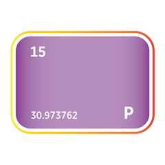
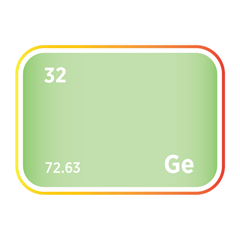
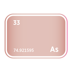
Phosphine (PH₃) and arsine (AsH₃) are critical n-type dopant sources in both silicon and III–V compound semiconductors such as gallium arsenide (GaAs) and indium phosphide (InP), supporting high-speed, optoelectronic, and RF applications. Diborane (B₂H₆) provides p-type doping capability and is also used in ion implantation for precise carrier concentration control. Germane (GeH₄) is used to deposit silicon–germanium (SiGe) epitaxial layers, enabling strain engineering that enhances carrier mobility in advanced logic nodes.
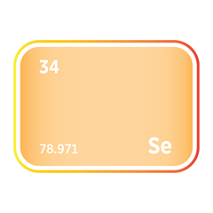
For II–VI semiconductor compounds, hydrogen selenide (H₂Se) and hydrogen telluride (H₂Te) act as key chalcogen precursors in the growth of materials like cadmium telluride (CdTe) and zinc selenide (ZnSe), which are used in infrared detection, photovoltaics, and optoelectronics.
Trimethylgallium (TMGa) and trimethylaluminium (TMA) are vital organometallic precursors in metal-organic chemical vapour deposition (MOCVD) processes. These compounds enable the controlled growth of gallium nitride (GaN), aluminium gallium nitride (AlGaN), and related alloys, which are foundational to high-power electronics, light-emitting diodes (LEDs), and next-generation RF devices.
These gases often incorporate elements such as hydrogen, nitrogen, phosphorus, germanium, arsenic, selenium, and tellurium. Their precise delivery, purity, and interaction with other process gases must be carefully managed to ensure atomic-level control of film composition, doping profiles, and crystal quality in highly sensitive semiconductor devices.
However, many of these compounds are also highly toxic, pyrophoric, or reactive, requiring robust containment, delivery, and abatement systems. Arsine, phosphine, and diborane are tightly regulated in most jurisdictions due to their acute health risks and dual-use potential. Supply is further complicated by the fact that production is concentrated among a small number of specialty gas firms based in the United States, Japan, Germany, and China. Export controls, hazardous materials regulations, and cross-border licensing regimes add layers of complexity to global sourcing.
As compound semiconductors become more strategically important to national security, photonics, defence, and next-generation wireless technologies, the secure and uninterrupted supply of high-purity speciality gases has become a growing area of concern. Countries with advanced semiconductor ambitions are investing in localised purification capacity, alternative precursor development, and diplomatic agreements to de-risk access to these essential but sensitive materials.


Meet the Critical Minerals team
Trusted advice from a dedicated team of experts.

Henk de Hoop
Chief Executive Officer

Beresford Clarke
Managing Director: Technical & Research

Jamie Underwood
Principal Consultant

Dr Jenny Watts
Critical Minerals Technologies Expert

Ismet Soyocak
ESG & Critical Minerals Lead

Thomas Shann Mills
Senior Machine Learning Engineer

Rj Coetzee
Senior Market Analyst: Battery Materials and Technologies

Franklin Avery
Commodity Analyst

Shunjie Zhao (Tony)
Commodity Analyst: APAC

How can we help you?
SFA (Oxford) provides bespoke, independent intelligence on the strategic metal markets, specifically tailored to your needs. To find out more about what we can offer you, please contact us.
