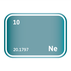
Neon
Critical Minerals and The Energy Transition
Navigating the Neon Market
Neon is a noble gas recovered in trace quantities, approximately 1 part per 65,000 from the fractional distillation of air, typically as a by-product of large-scale oxygen production at steel mills. Its remarkable inertness, high ionisation energy, and distinctive optical properties make it indispensable in a wide array of high-technology applications, including semiconductor photolithography, precision medical lasers, plasma displays, cryogenic cooling, and aerospace systems. Semiconductor fabrication is the dominant end-use, with ultra-high-purity neon critical to the excimer lasers that etch ever-smaller features onto silicon wafers. As chip complexity accelerates, so too does demand for neon. However, global supply has historically been concentrated in Ukraine and Russia, where production is tied to energy-intensive air separation units. Geopolitical risks and production bottlenecks have exposed vulnerabilities, prompting efforts to regionalise supply, enhance recycling, and invest in strategic reserves. New capacity is emerging in East Asia, North America, and the Middle East, but faces long lead times and high capital intensity. As neon’s role expands across semiconductors, defence, space, and quantum technologies, ensuring reliable access will be vital to supporting innovation, resilience, and industrial competitiveness.
An introduction to neon
Neon demand and end-uses
Neon plays a vital role across a wide range of high-technology applications, including semiconductor fabrication, laser-based medical systems, advanced lighting and displays, aerospace propulsion, cryogenic refrigeration, and scientific instrumentation. As demand accelerates from these sectors, neon is increasingly recognised as a strategically important and supply-sensitive element.
Its suitability stems from a combination of distinctive physical and chemical properties. Neon’s chemical inertness prevents oxidation and contamination in sensitive systems such as lasers, detectors, and vacuum environments. Its exceptionally high first-ionisation energy (21.6 eV) enables stable, high-voltage discharges and sharply defined emission lines, making it ideal for lighting and display technologies. Among noble gases, neon has one of the most intense discharge profiles, producing the ultraviolet pulses essential for excimer lasers used in semiconductor lithography and medical procedures. Its low atomic mass and high sound speed enable rapid energy transfer, supporting efficient performance in laser systems and micro-propulsion in aerospace. In cryogenics, neon delivers powerful refrigerating capacity between 25–50 K, ideal for cooling superconducting magnets and infrared sensors. Its unique spectral signature also enables ultra-sensitive leak detection and contributes to astrophysical measurements.
Semiconductor photolithography, the dominant demand driver, accounts for roughly 70% of global usage. Ultra-high-purity (6 N) neon forms the bulk of the ArF (193 nm) and KrF (248 nm) excimer-laser blends that etch sub-20 nm features on silicon wafers. Its inertness prevents contamination inside the laser cavity, while its low atomic mass supports rapid population inversion, enabling the high-energy ultraviolet pulses essential for advanced logic and memory chips.
-
Advanced Logic & Memory – CPUs, GPUs and 3-D NAND rely on neon-based lithography to achieve ever-smaller critical dimensions.
-
Foundry Expansion – new megafabs in Taiwan, South Korea, the United States and China are adding excimer-laser capacity, directly lifting neon demand.
Beyond chips, the same neon-rich laser blends power many medical and industrial excimer lasers:
-
Ophthalmology (LASIK & PRK) – 193 nm lasers reshape the cornea without thermal damage, delivering sub-micron accuracy for vision correction.
-
Dermatology & Aesthetics – Controlled ablation treats psoriasis, vitiligo, and scar tissue with minimal collateral heating.
-
Micro-machining & Texturing – Excimer beams pattern polymer films, print heads, and fuel-injection nozzles where mechanical tooling falls short.
Neon is used in lighting, signage and digitial display technologies. Although traditional neon signage ceded mass lighting to LEDs, the gas remains essential where its brilliant orange-red discharge or fast response is unmatched.
-
Architectural & Artistic Lighting – Custom neon tubes provide vivid colours and continuous lines that LEDs struggle to replicate.
-
High-voltage Indicators & Arrestors – Neon’s low breakdown voltage and visual feedback make it ideal for surge-protection devices.
-
Plasma & Flat-Panel Displays – Mixed with xenon in plasma cells, neon helps generate ultraviolet photons that excite screen phosphors.
-
LTPS Backplanes – Wide-beam excimer lasers anneal amorphous silicon into low-temperature polysilicon for OLED and high-resolution LCD panels.
In automotive and transportation safety, neon’s bright emission spectrum and ability to cut through fog and smoke support critical visibility applications:
-
Xenon-HID and Laser Headlamps – Neon participates in the arc-tube fill, delivering high luminance and long lamp life.
-
Railway Beacons & Aircraft Beacons – Steady, high-intensity red/orange output enhances safety in poor-visibility corridors.
-
Traffic Signals & Airfield Lighting – Stable colour coordinates and long operating life reduce maintenance cycles for public-safety infrastructure.
For cryogenic refrigeration and superconducting systems, liquefied neon offers about 40 times the volumetric cooling capacity of liquid helium, making it invaluable wherever compact, high-power refrigeration is required:
-
MRI Superconducting Magnets – Neon efficiently pre-cools helium circuits, cutting boil-off losses.
-
Infrared Detector Arrays – Space telescopes and military imagers use closed-cycle neon coolers to reach 30–50 K, suppressing thermal noise.
-
Particle-physics Bubble Chambers – Liquid neon offers high scintillation yield and fast electron drift for next-generation dark-matter detectors.
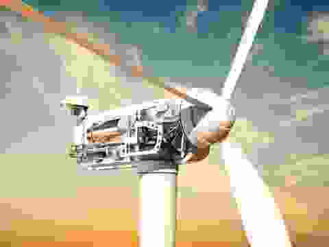
Space and aerospace technology represent another dynamic frontier, where Neon is gaining traction in specialised micro-propulsion and deep-space science, even as xenon continues to dominate large ion thrusters.
-
Hall-effect and ion Engines: Neon’s lower atomic mass yields higher exhaust velocity, which is advantageous for small satellite station-keeping.
-
Atmospheric & Solar Studies – Spectrometers aboard probes detect neon lines to infer stellar and planetary formation conditions.
In scientific research, analysis and leak detection, neon’s well-defined mass and thermal-conductivity profile are exploited in multiple ways:
-
Ring-Imaging Cherenkov Detectors – Ultra-pure neon fills long gas radiators, enabling precise particle identification at CERN and Fermilab.
-
Gas Chromatography & TCD – As a carrier gas, neon improves sensitivity when analysing light elements and isotope ratios.
-
Pipeline Leak Tracing – Minute neon injections, tracked by portable mass spectrometers, pinpoint underground natural-gas leaks within centimetres.
Finally, emerging and niche applications, continue to broaden neon’s horizon:
-
Quantum & Cryogenic Computing – Neon bath cryostats provide vibration-free cooling for superconducting qubit arrays.
-
Neon Ion Radiotherapy – Early clinical studies suggest enhanced tumour-control probability with reduced oxygen-enhancement ratios.
-
Hydrogen Production Catalysts – Plasma-assisted dry-reforming reactors use neon to stabilise arcs and extend electrode life.
With semiconductor, medical laser, space, and quantum technologies all expanding rapidly, neon will remain supply-sensitive and strategically vital. Diversifying production, investing in recycling, and building strategic reserves are essential steps toward securing future access to this irreplaceable industrial gas.

Strategic applications of Neon

Neon supply
The global neon supply chain is highly specialised, capital-intensive, and geographically uneven. For decades more than half of the world’s purification capacity sat in Ukraine, where large steel-mill air-separation units (ASUs) produced crude neon that two refiners upgraded to 99.999 % lithography grade. When Russia widened its invasion in February 2022, both plants stopped, instantly removing up to 54% of global semiconductor-grade supply and triggering a ten-fold price spike. The shock underscored a structural bottleneck: neon makes up just 0.0018 % of air, so only the largest ASUs (at least 1,000 t O₂ per day) can justify the deep-cold, multi-column distillation needed to harvest it.
With neon suddenly scarce following the loss of Ukrainian supply, every major chip-producing economy moved quickly to secure alternative feedstock and reduce dependence on vulnerable sources.
-
South Korea led the initial response, fast-tracking a domestic purification facility that came online in late 2022. The country also implemented a national recycling programme covering around 40% of in-fab neon demand, significantly easing pressure on imports.
-
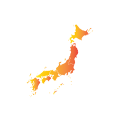
Taiwan is adopting a similar approach, installing purification systems at existing blast-furnace ASUs and targeting full local supply coverage by 2025. These efforts are designed to integrate neon production directly into the island’s industrial infrastructure, ensuring stable availability for its leading semiconductor manufacturers.
-
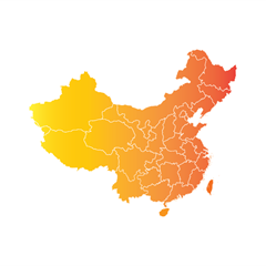
China, already operating the world’s largest fleet of air separation units, more than 40% of global capacity, is aggressively scaling up purification. State-backed incentives have enabled neon extraction to be bundled with broader industrial-gas projects, allowing new purification trains to be added to existing steel and petrochemical complexes. This integrated expansion supports China’s rapidly growing chip and display industries, reinforcing its position as a dominant supplier.
-
The United States, by contrast, remains a modest producer. A single vertically integrated operation draws crude neon from Midwestern ASUs and refines it at a dedicated facility on the East Coast. Additional ASU builds connected to Gulf-Coast petrochemical hubs are in development and could boost output later this decade. However, long qualification cycles—typically six to eighteen months per fab, continue to limit how quickly new sources can be adopted into critical semiconductor processes.
Geographic diversification is now being matched by rapid advances in closed-loop neon recovery. Tool-qualified recycling systems capture exhaust from excimer lasers, purify it back to six-nines (99.9999%) specification, and reintroduce it directly into the lithography process. These systems are already proving effective in reducing both supply risk and environmental impact.
At the fab level, leading memory producers have deployed plant-wide recycling units capable of reclaiming over 70% of process neon, with targets set to reach 77% by 2026. This lowers procurement costs significantly, saving tens of millions of dollars annually, and supports emissions reduction goals. Some systems, such as Cymer-qualified skids developed by specialist suppliers, can reduce scope 3 emissions by more than one million tonnes of CO₂ equivalent over a 20-year lifecycle. Recycling has thus emerged as a critical pillar of neon supply security, complementing regional production while aligning with broader sustainability objectives.
Strategic risk management now rests on three levers: stockpiles, multisourcing, and localisation or recycling to shorten supply lines. Key players in the chip sector typically hold about two months of neon inventory, and diversification after 2014 stripped roughly one-fifth of Ukraine’s earlier market share. Significant hurdles remain. The scarcity of neon limits where new purification hubs can be built, and lithography-grade quality control requires costly, long-lead analytical equipment. Lengthy certification cycles mean even qualified gas can sit idle for up to a year before full fab adoption. Looking ahead, supply resilience will depend on synchronising new ASU investments, scaling in-fab recycling, and maintaining rigorous qualification pipelines across every major chipmaking region.
Major neon producers


Other/emerging neon producers
Neon substitution
The 2022 disruption of Ukrainian neon supply exposed a significant vulnerability in the semiconductor industry’s reliance on excimer lasers, which depend on high-purity neon. With lithography accounting for around 70% of global neon use, particularly in 193 nm and 248 nm DUV processes, the war triggered a tenfold price spike. It intensified efforts to reduce or replace neon in chip manufacturing. In response, the industry is pursuing a multi-pronged strategy to mitigate neon risk. EUV lithography is expected to replace neon-intensive systems at advanced nodes, while solid-state laser technologies and nanoimprint lithography are being developed for broader applications. At the same time, improvements in recycling, strategic stockpiling, and supplier diversification are strengthening near-term resilience. Although complete independence from neon remains a longer-term goal, the industry’s coordinated response is already reshaping the landscape and steadily reducing exposure to one of its most fragile material inputs.
Looking ahead, the semiconductor industry’s approach to neon substitution is not singular but multi-pronged. EUV lithography will gradually displace neon-heavy systems at the leading edge, while solid-state and imprint techniques evolve for broader use. In the meantime, enhanced recycling, strategic stockpiling, and diversified sourcing safeguard continuity. Though complete neon independence remains distant, the industry’s coordinated response is steadily reducing its exposure to one of the most fragile links in the semiconductor value chain.
The most promising technological shift is the ongoing transition to Extreme Ultraviolet (EUV) lithography, which does not require neon. EUV systems generate 13.5 nm light using a tin plasma rather than gas discharge, marking a fundamental architectural departure from traditional excimer-laser-based DUV systems. Though EUV adoption was delayed for years, volume production began in 2019 and is now expanding rapidly at advanced nodes (7 nm, 5 nm, and below), with high-NA EUV tools currently under development. As EUV replaces DUV at the cutting edge, it offers a direct path to neon-free patterning, although DUV systems will likely persist in legacy and trailing-edge production for years to come.
In parallel, solid-state laser technologies are gaining ground as a potential replacement for neon-filled excimer lasers. Notably, Diode-Pumped Solid State (DPSS) lasers are being developed to generate DUV light at 193 nm—precisely the wavelength used in ArF excimer systems—without using toxic or noble gases. Recent breakthroughs from Chinese research institutions have demonstrated proof-of-concept systems using crystal-based laser media and advanced optics. While current output power remains below industrial thresholds (e.g. 70 mW vs 100–120 W for excimer systems), improvements in thermal management and power scaling may enable commercial adoption within the next decade. DPSS lasers offer operational advantages including reduced complexity, greater efficiency, and the elimination of routine gas handling and replacement.
Other alternatives are being explored as well. Nanoimprint lithography (NIL) bypasses the need for high-energy light altogether, using physical templates to mechanically press nanoscale patterns into photoresist. Multiphoton and interferometric lithography techniques—relying on ultrafast lasers and self-assembling materials—also present neon-free routes to high-resolution patterning, though they are not yet widely adopted at scale. Meanwhile, modified gas mixture strategies within excimer laser platforms continue to be studied, particularly the use of alternative noble gases like krypton, xenon, or argon, though these tend to introduce trade-offs in efficiency, pulse duration, or beam quality.
Despite their promise, most substitution technologies face significant performance, certification, and integration hurdles. Excimer lasers offer unparalleled beam stability and narrow-bandwidth emission, essential for the depth-of-focus and overlay precision required in semiconductor lithography. Replicating these characteristics with alternative technologies—especially at industrial scale and throughput—remains a major technical challenge. Moreover, any new system must undergo rigorous qualification processes that can take 6–18 months per fab, delaying implementation and limiting immediate substitution potential.
From an economic standpoint, alternatives like EUV and solid-state lasers demand significant capital investment in equipment and fab integration. However, long-term operational savings from reduced gas consumption, lower maintenance needs, and improved energy efficiency may offset initial costs. Neon recycling technologies are bridging the gap, allowing fabs to reduce procurement volumes and Scope 3 emissions while existing systems remain in place. These hybrid approaches, combining recycling, regionalised supply, and selective technology transition, are becoming the standard risk mitigation strategy across the industry.


Meet the Critical Minerals team
Trusted advice from a dedicated team of experts.

Henk de Hoop
Chief Executive Officer

Beresford Clarke
Managing Director: Technical & Research

Jamie Underwood
Principal Consultant

Dr Jenny Watts
Critical Minerals Technologies Expert

Ismet Soyocak
ESG & Critical Minerals Lead
Thomas Shann Mills
Senior Machine Learning Engineer

Rj Coetzee
Senior Market Analyst: Battery Materials and Technologies
Franklin Avery
Commodity Analyst

Shunjie Zhao (Tony)
Commodity Analyst: APAC

How can we help you?
SFA (Oxford) provides bespoke, independent intelligence on the strategic metal markets, specifically tailored to your needs. To find out more about what we can offer you, please contact us.