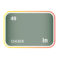
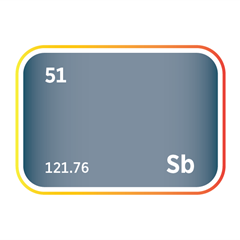
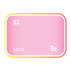
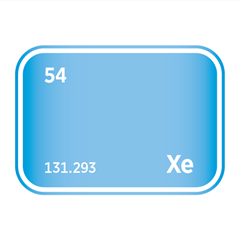
Semiconductors
Critical Minerals and Semiconductors
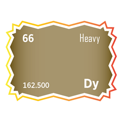
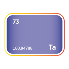
Semiconductors sit at the core of every modern electronic device, from smartphones and electric vehicles to cloud-scale AI accelerators. Their performance, efficiency, and longevity hinge on a small set of critical minerals whose unique physical and chemical properties enable precision transistor architecture, ultrafast signal transmission, and robust thermal management. Ultra-pure silicon wafers become the canvas for integrated circuits, doped with boron, phosphorus, and arsenic to sculpt nanoscale p–n junctions. Gallium, indium, and germanium expand the reach of high-speed, high-frequency, and optoelectronic components, while tantalum, tungsten, and cobalt reinforce interconnects that must move billions of electrons per second without degradation. Rare-earth elements such as neodymium and dysprosium enhance stepper lasers and high-strength magnets used in lithography and wafer handling, and copper, silver, and gold deliver low-resistance pathways for power and data. As chip geometries shrink toward the angstrom era and demand soars for AI-ready, energy-efficient processors, ensuring secure, sustainable supplies of these minerals becomes a strategic imperative. Disruptions, whether geopolitical, environmental, or technical, can ripple through entire technology value chains, stalling innovation and raising costs. Robust sourcing strategies, circular-economy recycling, and materials R&D are therefore essential to safeguarding the semiconductor ecosystem and, by extension, the digital technologies that drive global growth.
Critical Minerals used in semiconductors
Overview of Semiconductor Manufacturing
The semiconductor value chain can be understood not only as a linear process, but also through its functional categories, which define the material inputs, equipment technologies, and fabrication techniques that shape chip performance, yield, and supply chain exposure. The full manufacturing journey spans 32 discrete steps, from silicon crystal growth to final outbound logistics. These are grouped into seven functional domains, each with distinct strategic, technological, and material implications.
Below is an overview of these seven domains, including their associated process steps and strategic relevance:
1) Wafer formation & doping
Associated steps: 1, 2, 3, 4, 5, 6, 10
This phase lays the foundation for the entire semiconductor manufacturing process. It begins with the formation of high-purity silicon wafers and ends with the precise electrical tuning of their properties through doping. The accuracy achieved here directly impacts transistor performance, leakage control, and long-term device reliability. These steps create the substrate upon which every subsequent layer of the integrated circuit is built.
-
Step 1 – Silicon crystal growth: Ultra-pure polysilicon is melted in a quartz crucible and slowly cooled to grow a single-crystal silicon ingot. This is done using the Czochralski method, which yields defect-free crystals with tightly controlled electrical resistivity.
-
Step 2 – Ingot trim and grind: The ends of the ingot, known as the seed and tail, are trimmed to remove defects introduced at the beginning and end of crystal pulling. The ingot is then centre ground to achieve a uniform diameter. Orientation flats or notches are laser-scribed to mark the crystal axis for precise alignment in later steps.
-
Step 3 – Wafer slicing and edge shaping: The cylindrical ingot is sliced into thin discs using wire saws coated with synthetic diamond abrasives. These wafers are then edge-shaped to reduce stress concentrations and minimise the risk of breakage during handling.
-
Step 4 – Wafer flattening and polishing: The sliced wafers undergo chemical mechanical planarisation (CMP) to remove surface defects and achieve the flatness required for nanometre-scale patterning.
-
Step 5 – Epitaxial layer growth: A thin, defect-free, ultra-pure silicon layer is grown atop the wafer to improve electrical performance, particularly in advanced nodes.
-
Step 6 – Pad oxidation: A thin layer of silicon dioxide is thermally grown on the wafer surface. This oxide acts as an initial insulating barrier and protects the wafer during early lithography steps. This epitaxial layer enhances device performance, especially in advanced logic and power nodes, by providing a cleaner, more controlled starting surface.
-
Step 10 – Ion implantation and anneal: Specific dopant atoms, such as boron or phosphorus, are implanted into the wafer to tailor its electrical properties. A rapid thermal annealing process then activates these dopants and heals any crystal damage caused by implantation.
Together, these steps define the resistivity, carrier concentration, and mechanical integrity of the wafer. They set the baseline for electrical performance, thermal stability, and manufacturing yield across all downstream fabrication. Even minor deviations in dopant dose or crystal quality at this stage can compromise transistor function and chip reliability.
Key terms:
-
Polysilicon: Ultra-pure silicon made up of many small crystals, used as the feedstock for single-crystal growth.
-
Czochralski process: A technique for growing large single crystals of silicon by slowly pulling a seed crystal from molten silicon.
-
Doping: The addition of specific atoms to silicon to modify its electrical conductivity.
-
Epitaxy: The growth of a thin crystal layer that precisely matches the structure of the substrate underneath.
-
Annealing: A high-temperature treatment used to repair crystal damage and activate implanted dopants.
2) Active device layers
Associated steps: 8, 12, 13, 14
This section focuses on building the transistor structures that act as the active switching elements in integrated circuits. A transistor is a nanoscale electrical switch that controls the flow of current, enabling operations like logic processing, memory storage, and signal amplification. These fabrication steps define each transistor’s geometry, electrical characteristics, and conductive pathways. These steps are critical in determining the speed, power efficiency, and scalability of the transistor.
-
Step 8 – Fin or nanosheet fabrication and channel release: In advanced CMOS (complementary metal-oxide-semiconductor) nodes, transistors are formed using three-dimensional architectures. In FinFETs (Fin Field-Effect Transistors), channels are built as vertical fins of silicon to increase surface area and gate control. In newer gate-all-around (GAA) nanosheet devices, horizontal sheets are stacked and suspended above the wafer by selectively removing underlying sacrificial layers. These structures improve gate-channel contact and reduce current leakage. The process includes high-precision lithography, anisotropic etching of silicon, and channel release for nanosheet designs.
-
Step 12 – Spacer deposition and etch-back: A conformal dielectric film, often made of silicon nitride or silicon oxynitride, is deposited around the gate area. It is then anisotropically etched to form sidewall spacers. These thin insulating barriers define the lateral distance between the gate and the source/drain and play a crucial role in leakage control, electrical isolation, and implantation masking during later steps.
-
Step 13 – Source/drain epitaxy and junction engineering: Heavily doped semiconductor regions, known as source and drain, are grown selectively next to the transistor channel using epitaxial deposition. Materials like silicon-germanium (SiGe) or silicon-phosphorus (Si:P) are commonly used to introduce strain engineering, which enhances carrier mobility. The doping concentration and profile are carefully controlled to balance drive current, switching speed, and electrostatic integrity.
-
Step 14 – Silicidation: A thin metal layer, typically nickel (Ni), cobalt (Co), or platinum (Pt), is deposited onto exposed silicon in the source, drain, and gate areas. The metal reacts with the silicon to form a metal silicide, a low-resistance compound that significantly improves electrical contact between the silicon junctions and the overlying metal interconnects. This step is critical to reducing contact resistance and power loss.
As chipmakers move to ever-smaller nodes, this phase becomes increasingly important for delivering high-performance logic and low-power designs that meet modern application demands. These fabrication steps define the electrical switching behaviour of every transistor on the chip. The dimensions and material interfaces created here operate at scales below 10 nanometres, requiring sub-nanometre alignment accuracy. These challenges make this phase one of the most geometrically demanding in the semiconductor process and directly impact final device performance, leakage, and scaling potential at advanced technology nodes.
Key terms:
-
Transistor: A tiny switch that controls the flow of electrical current in a chip.
-
FinFET/nanosheet: 3D transistor designs that increase control over current and reduce leakage, enabling faster, more efficient devices.
-
Spacers: Thin insulating walls placed alongside the gate to precisely define the transistor’s structure.
-
Epitaxy: A technique for growing doped crystalline silicon in specific regions to form source and drain.
-
Silicide: A low-resistance compound formed by reacting metal with silicon to create better electrical contact.
3) Gate stack (high-k & ferroelectric)
Associated step: 11
The gate stack is one of the most important components in a modern transistor. It functions as the on/off switch, controlling how and when electrical current flows through the channel. In advanced semiconductor nodes, this structure is engineered using specialised materials that enable better performance, lower leakage, and higher energy efficiency.
Step 11 – Gate stack formation (high-k / metal gate):
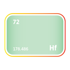
Historically, transistors used silicon dioxide (SiO₂) as the gate insulator and doped polysilicon as the gate electrode. However, as transistors became smaller, SiO₂ became too thin to prevent unwanted current leakage. To overcome this, modern gate stacks now use high-k dielectric materials, such as hafnium oxide (HfO₂) or zirconium oxide (ZrO₂), which offer superior insulation even at greater thicknesses. These high-k materials reduce leakage and allow continued transistor scaling.
Alongside the high-k layer, the gate’s conductive component is also upgraded. Instead of polysilicon, the gate electrode is now formed from metals like titanium nitride (TiN), tungsten (W), or ruthenium (Ru). These metals provide lower resistance, better compatibility with the high-k dielectric, and improved performance, particularly at smaller dimensions.
In the most advanced applications, the gate stack can also include ferroelectric materials, special oxides that retain their electric state even when power is removed. Ferroelectric-doped hafnium oxide, with elements such as lanthanum (La) or yttrium (Y), enables the creation of FeFETs (ferroelectric field-effect transistors). These devices combine the logic speed of traditional transistors with the data-retention capabilities of memory, making them attractive for embedded non-volatile memory and ultra-low-power logic.
The gate stack layer plays a decisive role in determining each transistor’s threshold voltage, leakage current, and switching efficiency, which are, key factors that define how fast and how power-efficient a chip will be. As scaling continues into the sub-5 nm range, gate stack engineering becomes more complex and even more essential to achieving node-to-node improvements in chip performance.
Key terms:
-
Gate stack: A layered structure in a transistor that controls the flow of current, essentially the transistor’s on/off switch.
-
High-k dielectric: An insulating material with high permittivity (ability to store electric charge), which blocks leakage current more effectively than silicon dioxide.
-
Metal gate: A conductive metal layer that replaces older polysilicon gates to improve switching speed and reduce electrical resistance.
-
Ferroelectric: A material that can hold an electric charge even when the power is turned off, enabling memory-like behaviour inside a transistor.
4) Interconnect & contacts (BEOL – Back-End-of-Line)
Associated steps: 15, 17, 20, 21
The BEOL defines the electrical pathways that allow millions to billions of transistors to function as a coherent integrated circuit. It includes both vertical interconnects (vias, contacts) and horizontal signal routing (metal layers). As chips scale down, the BEOL becomes more complex, requiring additional metal layers, finer features, and tighter spacing. Materials used here must offer excellent conductivity, electromigration resistance, and low signal delay, while remaining compatible with complex patterning, CMP, and barrier integration schemes.
This category encompasses the formation of both vertical and horizontal connections between transistors, as well as the redistribution of signals to external package interfaces. Once transistors are complete, they must be wired together into functional circuits. This is achieved during the BEOL, where a multilayer stack of metal interconnects, vias, and contacts is constructed above the silicon substrate. These connections define how signals travel between logic gates, memory blocks, and I/O pads, and are critical to the chip’s overall speed, power efficiency, and signal integrity.
-
Step 15 – Self-aligned contacts: Metal plugs are etched and filled to form vertical electrical pathways between the transistor terminals (source, drain, gate) and the first layer of wiring. These contacts are “self-aligned” to prevent shorts and maintain precise alignment with transistor features. They are typically made using tungsten (W) or cobalt (Co) and are lined with barrier materials such as titanium nitride (TiN) to prevent metal diffusion into surrounding dielectrics. Self-aligned contact structures are essential for minimising parasitic resistance and maintaining dimensional accuracy at advanced nodes.
-
Step 17 – Dual-damascene interconnects: This process builds the intricate, multi-level wiring that links all parts of the chip. This step forms the horizontal metal wiring layers that connect transistors across the chip, as well as the vertical vias that link successive layers. Using a technique called dual-damascene, both vias (vertical holes) and trenches (horizontal grooves) are etched into a low-κ dielectric material. These structures are then filled with copper (Cu), often lined with tantalum (Ta) or tantalum nitride (TaN), to form dense, low-resistance interconnects. The surface is polished flat using chemical mechanical planarisation (CMP). Multiple interconnect layers are stacked to form a high-performance signal routing network that handles data, clock, and power delivery.
-
Step 20 – Redistribution layers (RDL): RDLs are wide metal lines that reroute the fine internal connections to external bond pads. As a top-level metal routing layer built above the BEOL stack, the RDL repositions the chip’s internal wiring to match the wider pin pitch required by flip-chip, fan-out wafer-level packaging (FOWLP), or 2.5D interposer connections. These lines are typically made of copper, often plated with nickel and gold, and serve as the interface between the internal circuit and the chip package. Copper-based RDLs are used for these external-facing traces due to their high conductivity, corrosion resistance, and compatibility with solder bonding. RDLs are essential for chip-to-package alignment and are a critical enabler of high-density packaging and heterogeneous integration.
-
Step 21 – Backside metallisation: In power devices, image sensors, and high-performance logic, a metal layer—often titanium, tungsten, or copper—is deposited onto the back of the wafer. This layer provides electrical grounding, improves heat dissipation, and in some cases enables through-silicon vias (TSVs) for 3D stacking. Backside metallisation is increasingly important for thermal and power management, particularly in advanced nodes where layout density and heat flux are tightly constrained.
These steps govern resistance-capacitance (RC) delay, electromigration lifetime, and signal integrity, all of which are critical in high-density logic and memory designs. Material choices such as copper, cobalt, tantalum, and low-κ dielectrics, directly influence power delivery and circuit speed, making this one of the most performance-sensitive stages in chip manufacturing.
Key terms:
-
BEOL (Back-End-of-Line): This category encompasses the formation of vertical and horizontal connections between transistors, as well as redistribution of signals to the package interface.
-
Interconnects: Metal wires within the chip that carry signals between transistors and other circuit elements.
-
Vias: Vertical holes that connect different layers of metal wiring.
-
Dual-damascene: A fabrication technique that simultaneously creates both vias and horizontal trenches before metal filling.
-
Redistribution layer (RDL): A top-level metal layer that routes internal signals to external bonding sites.
-
Backside metallisation: Applying a metal layer to the wafer’s back to assist with grounding, thermal control, and vertical integration.
5) CMP, etch & cleaning
Associated steps: 7, 9, 16, 18, 19, 22, 23
This category includes key support processes that enable and maintain the precision required in advanced chip manufacturing. These steps are essential for shaping structures, removing unwanted materials, and keeping surfaces clean and flat throughout the front-end and back-end processes.
-
Step 7 – Shallow trench isolation (STI): To prevent electrical current from leaking between neighbouring transistors, narrow trenches are etched into the wafer and filled with an insulating oxide material. These filled trenches electrically isolate each transistor, preserving signal integrity and preventing short circuits. The surface is then polished to ensure a flat topography for the next patterning layers.
-
Step 9 – Photolithography: This is the process of transferring circuit patterns onto the wafer using light. The wafer is coated with a light-sensitive material called photoresist, then exposed to ultraviolet light through a patterned mask. After exposure, the photoresist is developed, and the underlying material is selectively etched to create the desired structures. This step is repeated dozens of times with different masks to define each circuit layer.
- Step 16 – Dielectric deposition (interlayer dielectric): Once the transistors are built, insulating materials called dielectrics are deposited between layers of metal interconnects to electrically isolate them. These insulators prevent short circuits and control parasitic capacitance. Low-κ dielectrics (materials with a low dielectric constant) are commonly used to reduce signal delay and improve energy efficiency in high-performance designs.
-
Step 18 – Chemical mechanical planarisation (CMP): As new layers are added during fabrication, the wafer surface becomes increasingly uneven. Chemical mechanical planarisation (CMP) uses a combination of chemical slurry and abrasive polishing to flatten each layer with nanometre-level precision. This planarisation is essential to maintain accurate focus in photolithography, ensure reliable metal patterning, and enable precise layer-to-layer alignment for advanced semiconductor structures.
-
Step 19 – Defect inspection and inline metrology: Throughout the manufacturing process, wafers are inspected using optical, X-ray, and electron-beam tools to detect defects such as particles, scratches, pattern misalignments, and thickness variations. In parallel, inline metrology tools measure critical dimensions, film thicknesses, and overlay accuracy at the nanometre scale to ensure each layer remains within specification. Early detection of these anomalies is essential for maintaining yield and preventing defects from propagating through subsequent process steps.
-
Step 22 – Wafer sort and electrical probe: After fabrication is complete, each individual die is electrically tested on the wafer using a probe card. This step, known as wafer sort, maps and records which dies pass or fail based on performance metrics. Good dies are marked electronically (inkless map), ensuring that only functional chips proceed to packaging.
-
Step 23 – Dicing / singulation: The wafer is cut into individual chips using a high-precision diamond saw or stealth laser dicing tool. Dicing must be exact to avoid chipping or cracking, which could compromise otherwise functional dies. Clean singulation is vital for achieving high packaging yields and long-term reliability.
These steps collectively ensure the structural integrity, pattern accuracy, and surface cleanliness required to maintain high manufacturing yield and chip performance. The extensive use of CMP, photolithography, and dry/wet etch processes makes this one of the most material- and consumable-intensive categories in the entire semiconductor process. These operations rely on high-purity chemicals, etchants, photoresists, abrasives, and inspection optics. Any error or contamination introduced here can propagate across layers, underscoring this stage’s importance in enabling successful lithography, interconnect formation, and final chip quality.
Key terms:
-
CMP (chemical mechanical planarisation): A technique that polishes surfaces to extreme flatness using chemicals and abrasives.
-
Photolithography: A light-based process for creating nanoscale circuit patterns onto a wafer.
-
Dielectric: An insulating material placed between metal layers to prevent short circuits.
-
Etch: A chemical or plasma-based process that removes selected materials from the wafer.
-
Wafer sort: Electrical testing of each chip on the wafer before packaging.
-
Dicing: Physically separating the wafer into individual chips.
6) Advanced packaging & assembly
Associated steps: 24, 25, 26, 27, 28, 29, 31, 32
Once a wafer has been processed and the individual chips have been tested and cut, they must be packaged. Packaging aims to protect the delicate chip, establish electrical connections to the outside world, and manage heat during operation. What was once a purely protective layer has now become a critical performance enabler, especially with the rise of 3D stacking, chiplets, and heterogeneous integration. This stage increasingly defines the performance envelope of modern chips, especially in advanced 2.5D and 3D architectures, where technologies like interposers, HBM (High-Bandwidth Memory), and chiplet-based design demand new packaging strategies. Material choices here directly influence electrical reliability, thermal conductivity, and integration density, making packaging a key differentiator in next-generation semiconductor devices.
-
Step 24 – Die attach: The individual chip (or "die") is physically attached to a package substrate or leadframe. This is typically done with an epoxy adhesive, conductive paste, or solder. The attachment method must provide both mechanical stability and good thermal conduction to pull heat away from the chip during operation.
-
Step 25 – Flip-chip attach / wire bond / micro-mump: This step forms the electrical connections between the chip and the package. There are multiple methods:
-
-
Wire bonding uses thin gold or copper wires to connect the die to the package pads.
-
Flip-chip bonding flips the die face down and connects it using solder bumps.
-
Micro-bumping is used in advanced 2.5D or 3D packaging to stack dies vertically with tiny interconnects.
-
-
Step 26 – Underfill and cure: For flip-chip packages, an underfill material is injected between the die and the substrate. This epoxy-based material protects the solder bumps from cracking during temperature changes and improves mechanical durability. After dispensing, the underfill is cured (hardened) in an oven.
-
Step 27 – Encapsulation or lid attach: The chip is sealed for protection using either:
-
-
Encapsulation involves moulding a plastic compound around the die.
-
Lid attach, often using a metal heat spreader for high-performance devices like CPUs or GPUs. This helps dissipate heat during operation.
-
-
Step 28 – Package back-grind and singulation: If the entire packaging process is done at the wafer level (known as WLP), the package stack is thinned by grinding from the back. This reduces thickness for mobile and compact applications. After thinning, individual packages are singulated (cut apart) for final handling.
-
Step 29 – Package test and burn-in: Each packaged chip is tested again under realistic operating conditions. Some devices are run through burn-in, where they operate at elevated temperatures and voltages for hours to screen out early-life failures. This helps ensure long-term reliability in the field.
-
Step 31 – Marking, tape-and-reel, or tray load: Functional chips are laser-marked with part numbers and lot information. They are then placed in trays or on reels, ready for high-speed assembly at electronics manufacturing plants.
-
Step 32 – Final quality control and outbound shipping: The finished, packaged chips undergo a final visual inspection and quality audit. They are vacuum-sealed in moisture-resistant packaging, often with desiccant and humidity indicators, and shipped to customers or contract manufacturers for board-level integration.
This stage has evolved far beyond physical protection. Advanced packaging now plays a decisive role in system performance, especially in AI, mobile, and high-bandwidth computing applications. Materials such as silver-filled die attach, low-CTE underfills, solder balls, polymer encapsulants, and metal lids are carefully selected to optimise thermal management, signal integrity, and mechanical durability.
Key terms:
-
Die: A single chip cut from the wafer.
-
Leadframe: A metal structure that supports the die and connects it to pins or solder pads.
-
Underfill: An epoxy that protects solder bumps and distributes mechanical stress.
-
Encapsulation: Protective sealing around the chip using plastic or epoxy resin.
-
Burn-in: Stress testing a chip to identify early failures before shipping.
-
Flip-chip: A packaging method where the die is flipped upside down and bonded using solder bumps.
7) Optical links, photonics & phosphors
Associated steps: 19, 30
While still a smaller share of the total manufacturing process, optical and photonic technologies are becoming increasingly important in advanced semiconductor applications. Traditionally, chips have relied solely on electrical signals. Still, new classes of devices now use or interact with light, whether to transmit data faster (optical interconnects), sense the environment (e.g. image sensors, lidar), or inspect critical features during manufacturing (optical metrology).
This category supports production-side inspection and system-level testing of chips that integrate light-based components. As data rates increase and electrical interconnects reach physical limitations, on-chip photonics, laser-based testing, and optical links become essential in sectors such as data centres, automotive vision systems, AI accelerators, and AR/VR.
-
Step 19 – Defect inspection and inline metrology (optical tools): In this step, advanced inspection systems use laser-based, X-ray, or electron-beam tools to detect defects in nanoscale chip structures. Many of these tools employ rare earth phosphors, such as gadolinium oxysulfide (Gd₂O₂S) or cerium-doped compounds, which convert radiation into visible light for detection. These phosphor-enhanced systems help identify missing lines, particles, voids, and pattern distortions in transistor layers and interconnect stacks. Without this high-resolution optical inspection, yield losses could go undetected until late in production.
-
Step 30 – System level test (SLT): SLT is the final functional test evaluates packaged chips under real-world conditions. This test ensures the chip operates correctly under expected workloads for devices incorporating photonics, such as silicon photonics transceivers, laser drivers, or optical sensors. Parameters such as laser alignment, photodiode sensitivity, optical I/O performance, and signal integrity are validated during SLT. This step is crucial for mission-critical applications in automotive cameras, lidar modules, AR/VR displays, and data centre switches, where failures cannot be tolerated.
As data speeds rise and traditional copper interconnects approach their physical and electrical limits, optical communication and on-chip photonics are emerging as critical next-generation solutions. These technologies enable faster, more efficient data transmission using light rather than electrical signals, reducing delay, power consumption, and crosstalk in high-density systems.
They rely on a growing set of specialised optical materials, including:
-
Germanium photodiodes for high-speed light detection
-
Indium phosphide (InP) lasers for optical transmission
-
Erbium-doped waveguides for light amplification within integrated circuits
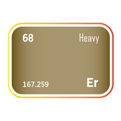
In addition, rare earth elements such as gadolinium (Gd), erbium (Er), ytterbium (Yb), and europium (Eu) play essential roles, both as phosphor dopants in metrology and as active optical materials in photonics-enabled chips. These materials are increasingly used in data centre interconnects, AI accelerators, image sensors, telecom modules, and immersive computing platforms at the edge.
Key terms:
-
Photonics: A technology that uses light (photons) instead of, or alongside, electrical signals for faster data transmission and sensing.
-
Optical Interconnect: A light-based connection between chips or systems that replaces or supplements traditional copper wires.
-
Phosphors: Materials that glow or convert radiation into visible light, used in imaging systems and inspection tools.
-
System-level test (SLT): A final, full-function test run on the chip after packaging, often using real firmware and workloads.
Key Manufacturing Steps, Minerals and their Roles
0) R&D / design (EDA & IP)
The semiconductor manufacturing process begins well before any wafer enters a fabrication facility. It starts at the R&D and design stage, where engineers define chip architecture using Electronic Design Automation (EDA) tools and integrate pre-built IP blocks—reusable circuit elements like memory controllers or CPU cores, typically licensed from vendors such as Arm, Synopsys, or Cadence. This work occurs in a virtual environment, akin to computer-aided design (CAD) for silicon, powered by high-performance computing (HPC) infrastructure running the intensive simulations required to validate functionality, optimise performance, and prepare final layouts for tape-out.
Although no wafers are physically processed at this stage, the infrastructure enabling design work is constructed from the very materials and technologies that will be deployed downstream. The servers, GPUs, and storage systems at the heart of the design environment contain silicon, copper, gold, and rare earth magnets, reflecting the broader material dependencies of the semiconductor ecosystem. Evaluation platforms and prototyping kits used during this phase further expand the mineral footprint, incorporating compound semiconductors such as gallium arsenide (GaAs), indium phosphide (InP), and germanium, as well as infrared-sensitive materials like cadmium telluride (CdTe) and cadmium zinc telluride (CdZnTe).
This stage offers a significant performance advantage through computational iteration speed. Scalable simulation environments allow engineers to test more design variants, optimise energy efficiency, and push clock speeds, all before committing to fabrication. Decisions made here, around architecture, process node, packaging, and IP integration, lock in downstream material and process dependencies. They determine whether a chip will be built on a silicon or compound substrate, and which critical materials, gallium, hafnium, cobalt, tantalum, and others, will become essential.
The design workflow relies on three interdependent tool categories:
-
Compute clusters form the hardware backbone of the design environment. These HPC platforms consist of multicore CPUs, high-end GPUs, and high-bandwidth memory arrays arranged in parallel server farms, delivering petaflops of processing power. This compute capacity is essential for simulating modern system-on-chip (SoC) designs, which may contain billions of transistors and require detailed modelling of thermal, electrical, and timing behaviours across both micro and macro scales.
Key materials:
– Silicon (Si): Forms the chips inside CPUs and GPUs.
– Copper (Cu), Gold (Au): Enable signal routing and power delivery across server motherboards.
– Rare Earths (Nd, Dy, Tb): Used in high-strength magnets found in fans and HDDs.
– Iron (Fe), Boron (B): Structural alloys and magnetic compounds in server infrastructure
-
IP libraries are pre-verified, reusable logic blocks that reduce development time and risk while ensuring compatibility with specific foundry nodes through Process Design Kits (PDKs). Though intangible, their use has tangible consequences: selecting a GaN power IP core points to future use of gallium, nitride, and silicon carbide (SiC); deploying silicon photonics IP implies the eventual need for germanium, erbium, or indium phosphide during fabrication.
Material implications:
– Selecting a GaN power IP core implies downstream use of gallium, nitride, and silicon carbide.
– Deploying silicon photonics IP signals likely incorporation of germanium, erbium, or indium phosphide.
-
EDA software suites are the tools used to create, simulate, verify, and finalise chip designs. Vendors like Synopsys, Cadence, Siemens EDA, and Ansys offer integrated platforms that cover:
– Logic design (HDL editing, RTL synthesis)
– Simulation (timing, thermal, EM, signal integrity)
– Verification (formal, functional, coverage)
– Physical design (place-and-route, design rule checking)
– Mask generation (GDSII export, optical proximity correction)
While software-driven, these tools dictate how physical materials such as hafnium, cobalt, tantalum, and low-κ dielectrics, are spatially arranged within the final chip. Design constraints encoded in EDA platforms govern minimum spacing, metal widths, and compatibility with process nodes, directly shaping future material usage.
The types of semiconductors defined during this stage, whether logic (CPUs, GPUs, AI accelerators), memory (DRAM, NAND), analogue/mixed-signal, or optoelectronic/sensor/discrete devices (OSD), further shape material requirements. For example, high-speed RF amplifiers and laser diodes are typically designed on compound semiconductor platforms such as GaAs or InP due to their superior optoelectronic properties, necessitating the use of gallium, indium, and arsenic. By contrast, most logic and memory chips remain silicon-based, though even these increasingly depend on advanced materials at smaller nodes to sustain performance scaling.
Ultimately, the design phase functions as a strategic control point in the semiconductor value chain. It does not directly consume raw minerals in fabrication volumes, but it defines which materials will be required, in what form, and at what scale. From process node selection and IP licensing to substrate choice and device architecture, every decision made at this stage influences downstream demand for critical elements such as gallium, hafnium, cobalt, tantalum, and others.
Despite being simulation-heavy and digital in nature, the design environment already relies on a wide array of physical materials. High-performance compute clusters are built on silicon processors and copper interconnects, with gold contacts and rare earth magnets supporting data storage and thermal systems. Evaluation boards and test vehicles introduce compound semiconductors such as gallium, arsenic, indium, and germanium, while imaging and sensor prototypes incorporate cadmium, tellurium, and gadolinium. These materials prefigure the mineral and materials footprint that the manufacturing process must ultimately fulfil.
Material usage in R&D environments
Though this stage is digital and simulation-heavy, the underlying hardware and prototyping platforms rely on a wide range of critical and strategic elements, many of which foreshadow the materials required in manufacturing:
-
Silicon – Silicon is the foundational material of modern electronics, underpinning everything from simulation servers to prototyping boards. It forms the basis of CPUs, GPUs, and DRAM used in the high-performance compute clusters that power EDA workflows. Its ubiquity in the design environment reflects its unmatched role across logic, memory, and analogue domains.
-
Copper – Copper provides the dense, low-resistance interconnects inside server motherboards, GPUs, and networking switches used in design environments. It carries power and signals within and between components and is vital to the thermal performance of large compute systems. Copper also appears in PCB traces, evaluation boards, and IP test platforms used during early design validation.
-
Gold - Gold is used in bonding wires, connector plating, and socket interfaces within HPC systems and prototyping environments. Its exceptional corrosion resistance and conductivity make it the metal of choice for reliable, long-life electrical contacts, ensuring stable performance in data centres, test jigs, and evaluation boards used in early-stage chip bring-up.
-
Neodymium – Neodymium, often alloyed with dysprosium and boron (as NdFeB), forms the permanent magnets in hard disk drives and high-torque cooling fans found in EDA compute clusters. These magnets enable compact, high-power motors that deliver the mechanical performance required for server-grade thermal and data storage systems.
-
Iron – Iron is a primary component in server chassis, magnetic cores in power inductors, and structural frameworks used in R&D infrastructure. In magnet alloys (e.g., NdFeB), iron contributes to the high saturation magnetisation essential for dense, efficient cooling fans and storage drives, critical for the uptime and thermal management of EDA clusters.
-
Boron – Boron plays a dual role in R&D environments: as a dopant in reference wafers or test chips used for process calibration, and as part of the NdFeB magnets in fan motors and HDDs. Boron enhances coercivity in magnets and is fundamental to p-type doping strategies that designers may explore virtually using TCAD and other device simulation tools.
-
Gadolinium – Gadolinium may appear in x-ray or thermal imaging prototypes evaluated during early device R&D. Its high neutron capture cross-section and unique magnetic properties make it a component of Gd₂O₃ or GdOS scintillators used in image sensors and inspection tools. Gd-based materials also appear in high-resolution diagnostic systems that support chip debugging.
-
Arsenic – Arsenic is a key dopant in III–V compound semiconductors like GaAs and InGaAs, which are frequently used on prototyping boards for RF, optical, and high-speed data applications. In R&D, test vehicles based on GaAs or InP substrates embed arsenic-rich compounds to enable fast switching and light emission—vital for validating IP used in photonics and RF front ends.
-
Indium – Indium is central to indium phosphide (InP) and indium tin oxide (ITO) technologies used in optical transceivers, laser drivers, and test vehicles for data communications. Design-stage platforms exploring photonic integration often include In-based materials, and indium-soldered optical components are commonly mounted on evaluation boards.
-
Germanium – Germanium plays an important role in SiGe test chips and prototype modules, especially where stress engineering or optical sensitivity is required. Early-stage performance validation for mixed-signal or photonic IP may use Ge-containing devices to explore high-speed behaviour, making Ge an indirect but strategic material in design-driven evaluation.
-
Tellurium – Tellurium appears in cadmium telluride (CdTe) and phase-change memory (GeSbTe) materials that are sometimes explored in emerging memory or IR sensor designs. Evaluation platforms for thermal imagers, edge AI sensors, or neuromorphic computing may use Te-containing chips, particularly in R&D centres focused on defence, medical, or aerospace applications.
-
Cadmium – Cadmium is used in CdTe and CdZnTe substrates for infrared detectors and X-ray imagers, technologies frequently evaluated in sensor-focused R&D labs. Cd-containing materials offer high quantum efficiency in long-wave infrared, making them key to early-stage prototyping for space, automotive, and surveillance applications.
The R&D and design phase is a critical upstream checkpoint where material footprints are implicitly defined. Through tool selection, IP licensing, and simulation choices, this stage determines what the fab will need and how the downstream supply chain must respond. It is the point where innovation and critical mineral demand first intersect.
EDA software suites: Core functions and material implications
EDA software suites are the central tools used to design, simulate, verify, and finalise semiconductor devices before fabrication. Developed by leading vendors such as Synopsys, Cadence, Siemens EDA, and Ansys, these platforms support the entire design flow, from high-level logic definition to physical layout and photomask preparation. Each stage within the suite has distinct responsibilities, and together they ensure the final chip design is functionally correct, manufacturable, and material-aware.
The five key domains of EDA functionality are outlined below, with further detail on how each contributes to the design process and influences downstream material demand:
1. Logic design (HDL editing, RTL synthesis)
Logic design is the first step in the digital design process, where engineers define the chip’s functional behaviour using hardware description languages (HDLs) such as Verilog or VHDL.
This begins with HDL editing, in which designers write code that describes how components like ALUs, memory controllers, or processor cores should behave, capturing logic operations, state transitions, and data flow. Once the high-level logic is defined, RTL (Register Transfer Level) synthesis converts it into a gate-level netlist, a map of logical elements such as flip-flops, multiplexers, and combinational gates. This netlist is then optimised for area, speed, and power.
Decisions made during logic design affect gate count, clock frequency, and power efficiency, all of which directly impact the physical die area, thermal load, and ultimately material demand in manufacturing, for instance, influencing the quantity of copper needed for interconnects or the use of hafnium-based high-κ dielectrics in transistor gate stacks.
2. Simulation (timing, thermal, EM, signal integrity)
Simulation assesses how a chip design will perform under real-world electrical, thermal, and physical conditions, long before it reaches silicon. This phase ensures that the design is not only functionally correct, but also electrically stable, thermally manageable, and signal-accurate at scale.
-
Timing simulation checks that signals propagate through logic paths within the bounds of a clock cycle, flagging any setup or hold violations that could cause functional errors.
-
Thermal simulation models how heat is generated and dissipated across the die, influencing layout decisions and the need for materials such as copper redistribution layers or indium-based thermal interface materials (TIMs) in packaging.
-
Electromagnetic (EM) simulation evaluates inductive and capacitive coupling between metal lines and components, identifying risks related to signal degradation, power integrity, or electromagnetic interference (EMI).
-
Signal integrity simulation ensures clean transitions along interconnects, detecting issues like glitches, overshoot, ringing, or crosstalk that can impair high-speed operation.
These simulation results directly inform the design of the power distribution network (PDN), routing strategies, and shielding requirements, factors that ultimately dictate the materials, thicknesses, and stack-ups used in the back-end-of-line (BEOL). From copper interconnects and low-κ dielectrics to barrier metals, simulation choices shape the physical material footprint of the chip.
3. Verification (formal, functional, coverage)
Verification is a strategic filter for resource efficiency, materially reducing the consumption of critical minerals and chemicals across the manufacturing process. It ensures that a chip behaves exactly as intended under all operating conditions, catching logic or design errors before fabrication begins. This stage provides functional correctness, logical completeness, and confidence that the design will operate reliably in real-world systems.
-
Formal verification uses mathematical techniques to prove that specific properties always hold—such as ensuring that a signal will never short, a register will always reset, or that illegal states are unreachable.
-
Functional verification relies on simulation and testbenches to validate that the design behaves as expected in practice, for example, confirming that a CPU core correctly executes instructions or that a peripheral interface responds to input in real time.
-
Coverage verification evaluates how comprehensively the logic has been exercised, measuring metrics like the percentage of branches, states, conditions, and paths that have been tested.
Together, these three verification methods form a critical safeguard against design flaws. Errors identified at this stage prevent costly mask re-spins, eliminate the risk of fabricating defective silicon, and avoid downstream waste of high-value materials such as photoresists, reticles, and ultra-pure wafers.
4. Physical design (place-and-route, design rule checking)
Physical design is the stage where a chip's logical structure is translated into a precise physical layout on a silicon wafer. It bridges abstract circuit behaviour with manufacturable geometries, defining the chip's physical footprint, interconnect architecture, and metal layer usage. It is a primary determinant of manufacturing cost and material efficiency.
-
Place-and-route (P&R) determines the location of logic blocks and routes the interconnects that link them. It specifies exact wire lengths, via placements, metal stack utilisation, and spatial relationships—factors that directly influence delay, power, and die area.
-
Design Rule Checking (DRC) ensures all layout geometries conform to foundry-defined manufacturing constraints, including minimum spacing, line width, overlay tolerances, and alignment rules for lithography and etch steps.
This phase is foundational to material consumption. It dictates the quantity and distribution of metals and dielectrics, such as copper, tungsten, cobalt, tantalum, hafnium, and low-κ materials, across the back-end-of-line (BEOL) stack. Strict DRC compliance is essential to avoid yield-limiting defects and lithographic failures, reduce rework, conserve high-value substrates, and minimise waste of critical materials during wafer processing.
5. Mask generation (GDSII export, optical proximity correction)
Mask generation is the final stage of the physical design process, where layout data is prepared for high-precision photolithography. It transforms a digital blueprint into a manufacturable form by producing the files and optical corrections required to guide mask fabrication and scanner operation.
-
GDSII export converts the verified physical layout into a standardised format used to fabricate photomasks. These masks define where specific materials—such as metals, dielectrics, and dopants—will be patterned, etched, or deposited on the wafer.
-
Optical Proximity Correction (OPC) adjusts geometric shapes in the layout to counteract distortions caused by diffraction and process limitations during lithography. Without OPC, features printed on silicon would deviate from their intended dimensions, particularly at advanced nodes.
OPC is indispensable at feature sizes below 10 nanometres, where EUV or ArFi lithography is required. More aggressive OPC results in greater pattern complexity, which in turn drives up the demand for advanced materials: molybdenum, chromium, and quartz for photomasks, and tin, ruthenium, and fluorine for scanner operation. Mask generation is thus a critical inflection point where data, optics, and material science converge, shaping both the precision of pattern transfer and the intensity of upstream mineral usage.
Stage 1) Silicon Crystal Growth (Monocrystalline Silicon Ingot)
Functional category: Wafer Formation & Doping (front-end substrate)
Step 1) Silicon crystal growth (monocrystalline silicon ingot)
Wafer fabrication is the heart of semiconductor manufacturing, where designed circuits are physically realised on silicon wafers inside a fabrication facility. This stage is capital- and materials-intensive, involving hundreds of discrete process steps and highly specialised equipment. A single chip may require over 500 manufacturing stages and depend on supply chains that cross dozens of international borders. Fabrication begins with the formation of the wafer itself, a precision-engineered substrate that underpins every layer of the integrated circuit.
Silicon wafers constitute the dominant substrate in modern semiconductors. Silicon is abundant in the Earth's crust, typically found as silica (SiO₂), but must be refined into ultra-high purity polysilicon before being grown into large single-crystal ingots. These ingots are the base material for all mainstream CMOS logic and memory chips. While alternative materials such as gallium arsenide or silicon carbide are used in specialised applications, silicon remains unmatched in performance-to-cost ratio, offering excellent carrier mobility, a high-quality native oxide, and mature process control.
The crystal growth process typically begins with 11N-grade polysilicon, which is melted in a high-purity quartz crucible. A seed crystal is then inserted and slowly pulled from the melt at approximately 1 mm per minute, forming a defect-free monocrystalline ingot, or boule, weighing between 150 and 450 kilograms. This is known as the Czochralski process, which dominates logic and memory wafer production. Float-zone growth is an alternative method used in niche high-voltage or high-resistivity applications where ultra-low contamination is required.
The Czochralski growth chamber is surrounded by an inert argon atmosphere, which prevents oxidation and contamination of the silicon melt. During the pull, minute quantities of dopants, typically boron, phosphorus, or arsenic, are introduced to control the wafer’s electrical properties. Boron (Group III) creates p-type material by generating holes, while phosphorus and arsenic (Group V) contribute electrons to form n-type material. These dopants establish the wafer’s baseline resistivity and carrier type, reducing the number and complexity of implantation steps required later in fabrication.
The quartz crucible contains the silicon melt and introduces trace oxygen levels into the crystal. While generally considered an impurity, oxygen at controlled levels strengthens the crystal lattice and creates internal gettering sites that trap metallic contaminants. The furnace assembly often incorporates graphite components to support the crucible and deliver heat. Some carbon from these elements may diffuse into the silicon at parts-per-billion levels, which can influence crystal defectivity but is often tolerated within control limits.
In some cases, nitrogen gas is introduced into the ambient environment to improve crystal quality. Nitrogen-doped silicon wafers exhibit reduced void defects, improved mechanical strength, and enhanced internal gettering performance. These attributes are particularly valuable in advanced CMOS nodes, where even sub-micron lattice irregularities can impact device yield.
The resulting single-crystal silicon ingot is cooled, extracted, and further processed. It is sliced into wafers, shaped, polished, and cleaned to meet the exacting standards required for front-end fabrication. The entire process is highly sensitive to impurity levels, thermal gradients, and mechanical stress. Any defect introduced at this stage carries forward through all subsequent manufacturing steps, making crystal growth one of the most critical control points in the semiconductor supply chain.
-
Silicon – Silicon is the foundational material for nearly all semiconductor devices. It is refined from quartz sand, or silicon dioxide, into high-purity polysilicon, which is then melted and grown into single crystals, typically by the Czochralski process. Silicon remains dominant due to its low cost, excellent native oxide (SiO₂), high charge carrier mobility, and a mature ecosystem of process control and tooling. These properties make it uniquely suited to high-volume CMOS manufacturing, outperforming III–V wafers in scalability and reliability for most logic and memory applications. In addition to these performance benefits, silicon is compatible with advanced lithography and doping techniques, making it essential for transistor scaling and dense integration. No other material combines electrical performance, mechanical robustness, thermal conductivity, and process maturity in the same way.
-
Oxygen - Oxygen is unintentionally but beneficially introduced into the silicon lattice during crystal growth, primarily from the quartz crucible. In trace amounts, oxygen atoms occupy lattice vacancies, which helps to stabilise the crystal structure and strengthen the wafer mechanically. More importantly, oxygen can create internal gettering sites, which are regions that trap metallic impurities and prevent them from affecting active device areas during later processing steps. This gettering capability is vital to device reliability, especially in high-performance and low-defect-yield nodes. Oxygen, although technically an impurity, functions as a structural enhancer and a defect management tool during both crystal formation and downstream fabrication.
-
Quartz (SiO₂) – Quartz is used to make the crucible that holds the molten silicon during the Czochralski pull. It is chosen for its chemical purity, thermal stability, and ability to withstand prolonged exposure to molten silicon at approximately 1,400 degrees Celsius. However, quartz also contributes trace amounts of oxygen impurities, on the order of 10¹⁸ atoms per cubic centimetre, to the growing crystal. This controlled oxygen incorporation is critical for wafer strength, dislocation suppression, and impurity gettering. As a result, quartz serves both a structural and chemical role, enabling the production of high-quality silicon ingots through its direct interaction with the melt and its containment function.
-
Dopant elements (B, P, As) – Controlled amounts of boron, phosphorus, and arsenic are introduced to define the electrical properties of the wafer from the outset. Boron, a Group III element, creates p-type silicon by introducing holes as majority carriers. Phosphorus and arsenic, both Group V elements, create n-type material by donating electrons. Doping the melt during crystal growth allows for precise control of resistivity and carrier concentration, reducing the number and complexity of later ion implantation steps. This approach also improves uniformity across the ingot, leading to better electrical consistency across dies and higher overall wafer yield. The dopant mix can be tailored to meet specific requirements, whether for low-leakage logic, fast-switching memory, or high-voltage power applications.
-
Inert gases (Ar) – Argon provides an inert atmosphere within the crystal growth chamber. By displacing oxygen and moisture in the ambient, argon prevents oxidation of the silicon melt and minimises contamination from air or furnace components. It also helps to maintain a stable thermal environment, which is essential for consistent ingot growth and uniform crystal quality. As a noble gas, argon is chemically inert, and its use ensures that reactive species are excluded from the environment, preserving the purity of both the melt and the growing crystal.
-
Graphite (C) – Graphite is used for furnace components such as heater coils, crucible supports, and insulation, due to its high-temperature stability and low chemical reactivity. While graphite is not intended to contribute to the melt composition, trace amounts of carbon can dissolve into the silicon at concentrations around 10¹⁷ atoms per cubic centimetre. If properly managed, this small amount of carbon can have neutral or even beneficial effects, such as contributing to lattice hardening or interacting with oxygen to stabilise dislocation structures. However, excess carbon can increase the risk of defect formation, so its presence must be tightly controlled through furnace design and ambient management.
Nitrogen (N) – Nitrogen is sometimes introduced into the ambient environment during crystal growth to improve crystal quality. Nitrogen atoms occupy interstitial sites in the silicon lattice, which can suppress the formation of voids, pin dislocations, and enhance the formation of internal gettering sites. Nitrogen-doped silicon wafers exhibit improved mechanical strength, better thermal stability, and reduced defect density, all of which contribute to higher yields in downstream fabrication. These properties are particularly valuable in advanced CMOS nodes and high-voltage applications, where even minor lattice irregularities can significantly affect device performance and long-term reliability.
Step 2) Ingot trim & grind (conditioning the crystal)
Once the monocrystalline silicon ingot has been grown and cooled, it undergoes a series of mechanical conditioning steps to prepare it for wafer slicing. The ingot is first trimmed to remove the seed and tail sections, which typically contain defects or irregularities introduced at the start and end of the pull. It is then centre-ground to achieve a uniform diameter, ensuring compatibility with automated wafer handling systems.
To establish orientation, one or more flats or notches are laser-scribed along the length of the ingot. These serve as reference points for every downstream tool, enabling correct wafer alignment during photolithography, doping, and etching steps. After grinding, the ingot may also undergo chemical edge etching and surface inspection to remove slip lines, dislocations, or surface defects, and to verify oxygen striation patterns. These inspections ensure the crystal meets strict structural and dimensional specifications before slicing begins.
The grinding process uses ultra-hard abrasive materials, primarily synthetic diamond and silicon carbide (SiC). Synthetic diamond, produced through high-pressure high-temperature (HPHT) or chemical vapor deposition (CVD) methods, is used for both trimming and centreless grinding wheels. Its extreme hardness enables sub-micron surface flatness and reduces the risk of micro-cracking at the wafer edge. Silicon carbide abrasives may also be used for intermediate grinding steps or edge bevel processing, offering a reliable and cost-effective complement to diamond-based tools.
Proper conditioning at this stage is critical to minimising mechanical stress and avoiding wafer breakage in later steps. A well-prepared ingot dramatically reduces handling-related yield loss and maintains geometric precision across the wafer batch, making this one of the key mechanical checkpoints in the wafer supply chain. When correctly executed, ingot trimming and grinding reduce total wafer breakage to only a few parts per million.
Diamond and silicon carbide (SiC) abrasives are essential materials used in the mechanical conditioning of silicon ingots due to their exceptional hardness and wear resistance.
-
Diamond (C) – Synthetic diamond, the hardest known material, is used in grinding wheels, wire saws, and slicing blades to achieve sub-micron surface precision during centre grinding, edge shaping, and wafer slicing. Its ability to maintain a sharp cutting profile under high load ensures consistent material removal rates, minimal chipping, and excellent surface flatness, all of which are critical to reducing defect propagation in later processing.
-
Silicon carbide (SiC) – Silicon carbide is also widely used as an abrasive material in semiconductor processing. Though softer than diamond, SiC offers an ideal balance of cutting power, thermal stability, and cost-effectiveness. It is commonly used in intermediate grinding steps, edge beveling, and surface conditioning, where slightly less aggressive abrasion is sufficient. SiC abrasives help remove damage layers from earlier mechanical operations and prepare the ingot for chemical etching and inspection. Its relatively low cost compared to diamond makes it especially valuable in high throughput grinding environments where abrasive wear is a factor. SiC supports precise material removal while helping to control surface stress and defect formation.
Stage 2) Wafer Slicing and Preparation (Ingot to Polished Wafer)
Functional category: Wafer Formation & Doping (front-end substrate)
Step 3) Wafer slicing & edge shaping
Once the monocrystalline silicon ingot has been trimmed and ground, it is sliced into thin wafers using high-precision cutting tools. The most common method is a multi-wire saw, where a continuous loop of fine wire coated with synthetic diamond abrasives moves through a slurry or abrasive fluid to slice the ingot into wafers approximately 675 micrometres thick. These wire saws offer minimal kerf loss, tight thickness control, and excellent surface quality. For smaller-diameter ingots, such as 150 mm, inner-diameter (ID) saws may still be used.
After slicing, wafers undergo edge shaping to chamfer and round the perimeter to a typical radius of 300 micrometres. This step reduces the formation of micro-cracks, suppresses bevel contamination, and improves mechanical strength during handling. Carefully controlling the bevel profile minimises stress concentrations that could otherwise lead to wafer breakage in later thermal or mechanical processing steps.
This stage relies on ultra-hard tools, particularly diamond-coated wires and precision edge grinders, to achieve sub-micron tolerances and clean surface finishes. The goal is to produce geometrically uniform wafers, mechanically robust, and ready for flattening and polishing in the next stage.
-
Diamond(C) – Diamond is the hardest known material and offers exceptional wear resistance, making it uniquely suited for slicing brittle materials such as silicon. In wafer manufacturing, synthetic diamond abrasives are bonded to wire saws and grinding tools to enable clean, efficient, and repeatable cutting. Diamond's hardness allows it to cut through silicon's crystal lattice without excessive tool wear or mechanical damage, enabling high dimensional accuracy and tight thickness control. Diamond-coated wires also minimise kerf loss, the material wasted during slicing, which helps maximise wafer yield from each ingot.
Additionally, diamond abrasives reduce mechanical vibration during cutting, which lowers the risk of introducing micro-cracks or subsurface damage that could affect wafer performance downstream. In the edge-shaping process, diamond grinding tools provide the precision needed to chamfer and round the wafer edge, a critical step for reducing stress concentrations, particle generation, and handling-related breakage. The extreme durability of synthetic diamond ensures consistent performance and long tool life, improving overall process stability and equipment uptime.
Step 4) Wafer flattening
After slicing, the silicon wafers must be flattened and polished to achieve the extreme surface planarity required for nanometre-scale lithography. This stage removes saw marks, topographic variation, and sub-surface damage, and ensures that each wafer is dimensionally uniform across its entire surface.
The process begins with double-side grinding, typically reducing 300 mm wafers to a target thickness of approximately 725 micrometres. This is followed by lapping, a mechanical abrasion process that improves parallelism between the wafer faces. Once the wafer is mechanically conditioned, it undergoes chemical mechanical planarisation (CMP) using slurries that contain colloidal silica (SiO₂), alumina (Al₂O₃), or ceria (CeO₂). CMP polishes the wafer to achieve a total thickness variation (TTV) of less than 0.2 micrometres and a surface roughness (Ra) below 0.12 nanometres. This level of flatness is necessary to maintain lithographic focus and overlay alignment across the entire die field.
Following CMP, wafers are cleaned using a sequence of wet chemical processes, including megasonic cleaning and RCA cleaning protocols such as SC-1 (NH₄OH + H₂O₂ + H₂O) and SC-2 (HCl + H₂O₂ + H₂O). These cleans remove particulate contamination, organic residues, and metallic ions, often reducing trace metal concentrations to below 0.06 parts per trillion (ppt). A final HCl rinse is often used to strip residual metal contaminants from the wafer surface.
This step is highly dependent on specialised consumables and toolsets, including CMP polishers, slurry delivery systems, and megasonic tanks. Abrasives such as ceria (CeO₂), a rare earth oxide, are preferred for their high oxide removal rates, while zirconia (ZrO₂) nanoparticles are used in later stages for high-k metal gate polishing. Other critical chemicals include hydrofluoric acid (HF), potassium hydroxide (KOH), and chlorine-based etchants.
-
Silicon Dioxide (SiO₂) – Silicon Dioxide (SiO₂) is a widely used abrasive in chemical mechanical planarisation (CMP) slurries. Its fine particle size and relatively low hardness allow for gentle, uniform polishing of silicon wafer surfaces, particularly during oxide removal steps. SiO₂ provides a balanced removal rate and low defectivity, making it ideal for applications where surface planarity and minimal damage are critical.
-
Aluminium Oxide (Al₂O₃) – Aluminium Oxide (Al₂O₃) serves as both a CMP abrasive and a lapping medium. Harder than silicon dioxide, Al₂O₃ is used when more aggressive material removal is needed, such as during initial flattening or in cases where tougher layers must be planarised. Its high mechanical durability also makes it effective in earlier grinding stages and when processing harder dielectric stacks.
-
Ceria (CeO₂) – Ceria (CeO₂) is a high-performance abrasive that offers the fastest oxide removal rates among CMP materials. It is especially effective at polishing thermal silicon dioxide and is crucial for achieving Ångström-level surface flatness. As one of the few rare earth compounds used in front-end semiconductor processing, ceria is valued for its high oxide-to-silicon selectivity, low defectivity, and its ability to maintain tight process control at advanced nodes.
-
Zirconium Oxide (ZrO₂) – Zirconium Oxide (ZrO₂) is a nanoparticle abrasive used in the planarisation of high-k dielectrics and metal gate stacks, particularly in advanced logic nodes. Though not a rare earth element, ZrO₂ behaves similarly in nanoscale form, offering excellent control and low scratch rates during high-precision CMP steps. It is commonly used in polishing processes for high-k metal gate (HKMG) structures, where defect-free surfaces are essential.
-
Hydrofluoric Acid (HF) – Hydrofluoric Acid (HF) is a powerful wet etchant used to remove native oxide films from silicon surfaces. Following CMP, residual silicon dioxide layers must be eliminated to prepare the wafer for further processing steps such as epitaxial growth or dielectric deposition. HF’s selectivity and reactivity make it indispensable for final cleaning and surface conditioning.
-
Potassium Hydroxide (KOH) – Potassium Hydroxide (KOH) functions as both an etchant and a cleaning agent in wafer processing. It anisotropically etches silicon, creating well-defined surface features for MEMS or trench structures, and is also used in combination with oxidisers and surfactants for precision cleaning. Its compatibility with silicon surfaces makes it a useful component in both batch and wet bench cleaning processes.
-
Chlorine (Cl) (in HCl rinse) – Chlorine (Cl), often delivered via hydrochloric acid (HCl), is used to remove residual metallic contaminants from wafer surfaces. Chlorine forms volatile metal chlorides with trace elements like iron and copper, allowing them to be rinsed away. This step is critical for achieving ultra-low metal ion levels before device fabrication begins, preventing electrical leakage and reliability issues.
-
Water (H₂O) – Water (H₂O) is the universal solvent in semiconductor cleaning and slurry systems. It serves as the carrier for etchants, cleaning agents, and abrasives, and plays a vital role in controlling chemical concentrations, cooling reaction zones, and flushing away residues. Ultrapure water (UPW) is used throughout the process to maintain strict contamination control.
Stage 3) Front-End-of-Line (FEOL) – Transistor Fabrication
Functional categories: Wafer Formation & Doping, Active Device Layers, Gate Stack (High-k & Ferroelectric)
Step 5) Epitaxial layer growth
In this step, a thin, defect-free crystalline layer is grown on top of the silicon wafer surface. This epitaxial layer, or "epi", serves as the foundation for high-performance transistor channels in advanced CMOS nodes, and is also critical for power, analogue, and radio frequency (RF) devices requiring low-defect active layers.
The process typically uses reduced-pressure chemical vapour deposition (RPCVD) or low-pressure CVD (LPCVD) systems operating between 650°C and 1,050°C. During deposition, gases such as dichlorosilane (SiH₂Cl₂), hydrochloric acid (HCl), germane (GeH₄), and sometimes deuterium (D₂) are introduced to form layers of silicon (Si), silicon-germanium (Si₁₋ₓGeₓ), or other compound semiconductors. The result is a highly controlled film with precisely engineered composition and lattice strain, often 10–30 nanometres thick for Si caps or 20–40 nanometres for SiGe.
Strain engineering is a central goal of epitaxy at advanced nodes. By adjusting the germanium or carbon content, engineers can induce tensile or compressive strain in the channel region, improving carrier mobility and overall transistor performance. For example, SiGe layers introduce compressive strain for PMOS, while Si:C (carbon-doped silicon) creates tensile stress for NMOS. Materials like GeSn are being explored for high-mobility p-type field-effect transistors (PFETs) in more advanced applications.
In specialty applications, epitaxy grows II–VI semiconductor compounds such as cadmium telluride (CdTe) or cadmium zinc telluride (CdZnTe). These materials are essential for infrared detectors, X-ray sensors, and other optoelectronic systems. Additionally, deuterium (D₂) is now used in some gate-last process flows to passivate hot-carrier traps, significantly improving long-term reliability.
-
Silicon – Silicon is the foundational element for epitaxial growth in most semiconductor devices. In Step 5, epitaxial silicon layers are grown atop the wafer to create ultra-pure, low-defect starting surfaces for transistor formation. This enables precise doping control, reduces crystal dislocations, and improves junction isolation. In advanced logic nodes, ultra-thin Si layers are also used as caps above strain-engineered layers to protect the channel and enhance mobility.
-
Germanium – Germanium is incorporated into epitaxial layers to form silicon-germanium (SiGe) alloys, which induce compressive strain in p-type (PMOS) transistor channels. This strain improves hole mobility, resulting in faster switching and lower drive voltage. In addition, germanium is used in high-mobility GeSn alloys for emerging PFET channels, particularly in sub-5 nm nodes and advanced FinFET or nanosheet architectures.
-
Hydrogen - Hydrogen is a standard component in CVD gas flows, acting as a carrier gas, surface passivator, and etch modulator. During epitaxy, hydrogen helps prevent unwanted oxide formation, promotes smooth crystal growth, and assists in removing volatile by-products like SiCl₄. It also terminates dangling bonds at the surface, improving epitaxial layer quality.
-
Chlorine – Chlorine is introduced as hydrochloric acid (HCl), which serves multiple purposes in epitaxy. It etches excess silicon, helps maintain a smooth surface, and removes contaminants during the growth cycle. Chlorine reacts with unwanted impurities to form volatile chlorides that can be purged from the chamber, resulting in ultra-clean, defect-free layers.
-
Carbon – Carbon is added to epitaxial silicon to form Si:C stressors, introducing tensile strain into n-type (NMOS) transistor channels. This tensile strain enhances electron mobility, improving switching speed and reducing resistance. Carbon’s small atomic radius allows it to substitute into the silicon lattice without excessive defect generation, making it a precise strain-engineering tool for high-performance logic devices.
-
Tin – Tin is used in germanium–tin (GeSn) alloys for next-generation p-type channels. Adding tin to germanium reduces the bandgap and enhances hole mobility, making GeSn attractive for high-performance PFETs. Sn incorporation enables lower power operation and compatibility with future nanosheet or vertical device architectures.
-
Cadmium – Cadmium is used in compound semiconductor materials like cadmium telluride (CdTe) and cadmium zinc telluride (CdZnTe) grown epitaxially for infrared sensors and X-ray detectors. Cd enables high absorption efficiency and sharp energy resolution, making it essential for imaging and optoelectronic applications that demand precise material control.
-
Tellurium – Tellurium is combined with cadmium to form CdTe or CdZnTe epitaxial films. These II–VI semiconductors have excellent optical properties and are ideal for infrared, X-ray, and thermal imaging sensors. Te contributes to high carrier mobility and spectral sensitivity, especially in long-wavelength detection applications.
-
Zinc – Zinc is often alloyed with CdTe to form CdZnTe, a tunable material for high-resolution photodetectors. Zinc helps adjust the bandgap and mechanical properties of the crystal, improving detector efficiency and compatibility with integration schemes. Zn also enhances lattice matching and reduces dislocation density in the final epitaxial layer.
-
Deuterium – Deuterium, a heavy isotope of hydrogen, is increasingly used in advanced gate-last process flows following epitaxial growth. When incorporated into the silicon lattice or gate stack, deuterium is more stable than hydrogen and effectively passivates hot-carrier traps, significantly enhancing device reliability. It is vital in ultra-scaled transistors where stress-induced leakage and charge trapping can degrade performance over time.
Step 6) Front-side oxidation / pad oxide
In this step, a thin layer of silicon dioxide (SiO₂) is thermally grown on the silicon wafer surface to serve as a sacrificial or pad oxide. This layer acts as an initial insulating barrier, protects the wafer during early lithography steps, and supports isolation mask formation for defining active device regions. The pad oxide is critical for advanced logic and power nodes, providing a clean, controlled surface that enhances device performance by reducing defects and contamination.
The process typically employs oxidation furnaces operating at 800–1100°C, using dry oxygen (O₂) or wet steam (H₂O) to grow a 5–20 nm SiO₂ layer. Dry O₂ oxidation is preferred for its precise control over thickness and uniformity, producing a high-quality dielectric with minimal impurities. The reaction (Si + O₂ → SiO₂) consumes silicon from the wafer surface, simultaneously smoothing epitaxial defects and gettering residual metallic contaminants, which improves surface quality and device reliability. Wet oxidation with H₂O may be used for thicker layers when speed is prioritised over precision.
Oxygen (O₂) is the key reactant in this step, enabling the formation of a dense, uniform SiO₂ layer with excellent insulating properties. This layer isolates active regions, preventing unwanted electrical interactions, and serves as a cushion for subsequent processing steps, such as nitride deposition or ion implantation. The precise control of O₂-based oxidation ensures the thin pad oxide meets the stringent requirements of advanced nodes, where even minor variations can impact yield and performance.
In some process flows, the pad oxide also facilitates strain engineering by providing a stable base for subsequent layers, such as silicon nitride, used in shallow trench isolation (STI). The SiO₂ layer's ability to passivate the surface further enhances long-term device reliability by reducing leakage currents and improving junction isolation.
-
Oxygen – Oxygen is the foundational element for thermal oxidation in this step. O₂ reacts with the silicon wafer to form a high-quality SiO₂ pad oxide layer, insulating surface that protects the chip, reduces defects, and sets the stage for building advanced semiconductor devices.
Step 7) Shallow-trench isolation (STI)
Narrow trenches, or “moats”, are etched into the silicon wafer and filled with insulating oxide to electrically separate transistors. This process prevents unwanted current leakage between neighbouring devices, ensuring clear signals and avoiding short circuits. It’s vital for modern chips, especially at advanced nodes like 7 nm, where precise isolation enhances performance and reliability.
The process starts with etching 100–400 nm deep trenches using inductively coupled plasma (ICP) etching for high accuracy. A thin 5 nm silicon nitride (Si₃N₄) layer lines the trenches as a barrier, followed by filling with high-density plasma (HDP) oxide for excellent insulation. The surface is then polished using chemical-mechanical planarisation (CMP) back to the pad nitride layer, creating a flat, smooth surface for further patterning. This achieves ultra-low leakage currents, less than 5 fA µm⁻¹, at 7 nm nodes. For advanced memory chips like 3-D NAND, boron nitride (BN) masks are used instead of silicon nitride (SiN) due to their superior resistance to high-density plasma etching, ensuring precise trench formation in complex structures.
Silicon, oxygen, nitrogen, fluorine, and boron each play key roles in creating these insulating barriers, contributing to the precision and performance of advanced semiconductor devices.
-
Silicon – Silicon forms the wafer’s foundation, providing the base material into which trenches are etched. Its crystalline structure supports precise etching and subsequent filling, creating well-defined isolation regions critical for transistor performance in advanced semiconductor devices.
-
Oxygen – Oxygen is key to forming the high-density plasma (HDP) oxide that fills the trenches. This insulating oxide layer prevents electrical leakage between transistors, ensuring reliable device operation and supporting the high performance required in modern chips.
-
Nitrogen – Nitrogen is used to create the thin silicon nitride (Si₃N₄) layer that lines the trenches. This layer acts as a robust barrier, enhancing the structural integrity of the isolation and protecting the silicon during the oxide filling process.
-
Fluorine – Fluorine plays a crucial role in the ICP etching process, enabling precise and controlled removal of silicon to form trenches. Its reactivity ensures clean, sharp trench profiles, essential for effective isolation in advanced nodes.
-
Boron – Boron is incorporated into boron nitride (BN) masks, particularly important for 3-D NAND STI. BN’s superior resistance to high-density plasma etching compared to SiN ensures durable, accurate trench formation in complex, high-aspect-ratio structures.
The main toolsets include HDP chemical vapour deposition (CVD) for oxide filling and CMP for surface polishing, which ensure a high-quality, planar surface for subsequent processing steps.
Step 8) Fin / nanosheet fabrication & channel release
Three-dimensional structures called fins or nanosheets are crafted to build transistors in advanced chips, such as FinFETs (Fin Field-Effect Transistors) or gate-all-around (GAA) devices. These structures increase the gate’s contact area with the transistor channel, improving control and reducing current leakage. This is vital for high-performance chips at 3 nm or 2 nm nodes, where efficiency and speed are critical.
The process begins with high-precision extreme ultraviolet (EUV) lithography to pattern the wafer, followed by anisotropic etching to carve 20–35 nm tall silicon fins. For GAA nanosheet designs, alternating layers of silicon (Si) and silicon-germanium (SiGe) are etched selectively using a mix of hydrochloric acid (HCl) with oxygen (O₂) or nitrogen dioxide (NO₂) to release stacked nanosheets, creating suspended horizontal sheets. A combination of hydrogen bromide (HBr) and chlorine (Cl₂) gases ensures smooth, vertical fin profiles during reactive ion etching (RIE). These steps result in precise, high-performance transistor channels.
Silicon, germanium, hydrogen chloride, fluorine, chlorine, and bromine each play vital roles in sculpting these advanced structures, enabling chips to be faster and more efficient.
-
Silicon – Silicon is the main material for forming fins or nanosheets, providing the base for transistor channels. Its crystalline structure allows precise etching to create tall, narrow fins or thin sheets, essential for high-performance transistors in advanced chips.
-
Germanium – Germanium is used in silicon-germanium (SiGe) layers for nanosheet designs. These layers are selectively etched away to release the silicon nanosheets, enabling the gate-all-around structure that enhances transistor control and efficiency.
-
Hydrogen Chloride – Hydrogen chloride (HCl) is crucial for selectively etching silicon-germanium layers in nanosheet fabrication. Combined with oxygen or nitrogen dioxide, it carefully removes sacrificial layers, freeing the nanosheets for gate-all-around designs.
-
Fluorine – Fluorine is used in etching processes to precisely shape silicon fins or nanosheets. Its high reactivity ensures clean, accurate cuts, which are critical for creating the tiny, uniform structures needed in advanced nodes.
-
Chlorine – Chlorine, often mixed with hydrogen bromide (HBr/Cl₂), helps etch smooth, vertical fin profiles during reactive ion etching. This precision is key to forming consistent, high-quality fins for FinFET transistors.
-
Bromine – Bromine, combined with chlorine in HBr/Cl₂ mixtures, enhances control over etching to produce smooth, straight-sided fins. This ensures reliable transistor performance by maintaining precise structural shapes.
Main toolsets include EUV lithography for patterning and atomic layer etching (ALE) for precise material removal, ensuring accurate and consistent fin and nanosheet formation.
Step 9) Photolithography cycle
Circuit patterns are transferred onto the silicon wafer using light in a repeating process called photolithography. This step, repeated over 100 times, shapes the tiny features of modern chips, ensuring precise circuit layouts for high-performance devices at sub-30 nm scales.
The process starts by spin-coating the wafer with a light-sensitive material called chemically amplified photoresist. The wafer is then exposed to extreme ultraviolet (EUV) light at 13.5 nm or deep ultraviolet (DUV) light at 193 nm using argon fluoride (ArF) immersion systems through a patterned mask. After exposure, a post-exposure bake strengthens the pattern, followed by developing and rinsing the photoresist to reveal the circuit design. For features smaller than 26 nm, techniques like self-aligned double or quadruple patterning, or EUV multi-pass, are used to achieve ultra-fine pitches. These steps define each layer of the chip’s complex circuitry.
Specialised gases (neon, argon, krypton, xenon, fluorine, and selenium in the form of selenium hexafluoride) and other materials (tin, calcium fluoride, chromium, molybdenum, silicon, tantalum, erbium, and ytterbium) each play critical roles in creating precise patterns, enabling faster, more efficient chips.
-
Neon – Neon is used in excimer lasers for 193 nm DUV lithography, where DUV stands for deep ultraviolet. Its inert nature, meaning it doesn’t easily react with other substances, and its ability to emit stable, high-energy light when excited ensure consistent laser performance. This ensures precise patterning of circuit features across multiple chip layers, critical for high-volume production.
-
Argon – Argon is a key component in argon fluoride (ArF) lasers for 193 nm DUV lithography. Combined with fluorine, it produces high-energy light to pattern fine circuit details, supporting the high-resolution needs of advanced nodes like 7 nm, where precision is vital for chip performance.
-
Krypton – Krypton is used in krypton fluoride (KrF) excimer lasers, often at 248 nm, though still relevant in some DUV processes. When paired with fluorine, it emits specific ultraviolet wavelengths, ensuring accurate patterning. Its high atomic mass contributes to stable laser output.
-
Xenon – Xenon is used in EUV lithography systems to capture flare data, reducing light scattering errors. Its high atomic number enhances sensitivity to EUV light, improving pattern accuracy at 13.5 nm, critical for sharp, defect-free circuits in 3 nm or 2 nm nodes.
-
Fluorine – Fluorine, an electronic gas, is essential in excimer lasers (ArF or KrF) for DUV lithography, producing ultraviolet light with argon or krypton. Its high reactivity enables sharp, high-resolution patterning, critical for defining the tiny features of advanced chip designs with minimal errors.
-
Selenium – Selenium, in the form of selenium hexafluoride (SeF₆), an electronic gas, is used for eco-friendly photoresist stripping in EUV lithography lines. It efficiently removes residual photoresist after patterning, ensuring a clean wafer surface without environmental harm, critical for sustainable manufacturing.
-
Tin – Tin creates a plasma that generates 13.5 nm EUV light. Its electronic structure allows it to emit extreme ultraviolet radiation when laser-heated, enabling ultra-fine patterning below 7 nm, vital for the nanoscale accuracy of advanced chips.
-
Calcium Fluoride – Calcium fluoride (CaF₂) is used in lenses for EUV and DUV lithography due to its high transparency to ultraviolet light and low refractive index, which minimises light bending. These optical properties ensure precise light focusing with minimal distortion, enabling accurate pattern transfer.
-
Chromium – Chromium is applied as a thin layer on photomasks, forming opaque regions that block light during exposure. Its high opacity and resistance to wear ensure sharp, durable patterns during exposure, maintaining circuit integrity across multiple lithography cycles for consistent chip production.
-
Molybdenum – Molybdenum is used in EUV photomasks, forming reflective multilayer stacks with silicon for 13.5 nm light. Its high reflectivity and thermal stability, resisting deformation under heat, enable precise light guidance, and support ultra-fine patterning at 3 nm or 2 nm nodes.
-
Silicon – Silicon is the wafer’s base, providing a smooth, crystalline surface for photoresist coating and etching. Its uniform lattice structure ensures accurate pattern transfer, supporting reliable circuit formation across all chip layers in complementary metal-oxide-semiconductor (CMOS) processes.
-
Tantalum – Tantalum is used in EUV photomask absorbers, blocking specific areas of 13.5 nm light to create precise patterns. Its robust absorption properties and resistance to wear ensure consistent, high-quality patterning for advanced nodes, maintaining chip reliability.
- Erbium – Erbium is doped into lasers and waveguides for silicon-photonic mask levels, used in chips with optical components. Its strong light amplification at specific wavelengths enhances patterning precision for photonic circuits, critical for optical communication in advanced chips.
-
Ytterbium – Ytterbium is doped into lasers and waveguides for silicon-photonic applications. Its effective light amplification via electronic transitions supports precise patterning of photonic circuits, improving performance in chips designed for optical signal processing.
Main toolsets include EUV lithography systems for 13.5 nm patterning, ArF immersion (ArFi) for 193 nm DUV, and resist tracks for coating, baking, and developing photoresist, ensuring precise and repeatable pattern transfer across dozens of chip layers.
Step 10) Ion implantation
Specific atoms are fired into the silicon wafer to change its electrical properties, making it more or less conductive in precise areas to form transistor components. This step, followed by a quick heat treatment, ensures the atoms are activated and any damage to the silicon’s structure is repaired, which is vital for high-performance chips at advanced nodes like 7 nm or below.
The process uses ion implanters to shoot atoms like boron (B), phosphorus (P), arsenic (As), or antimony (Sb) into the wafer at low energies of 0.2–3 keV (kilo-electron volts, a measure of energy), with a 7° tilt and 360° rotation to ensure even distribution. A rapid thermal processing (RTP) step, called spike anneal, heats the wafer to 1,050–1,100°C for 0.1–0.3 seconds to activate the dopants, making them part of the silicon’s crystal structure, while keeping junctions (boundaries between doped regions) shallow at ≤8 nm. Additional materials like helium (He), carbon (C), and germanium (Ge) assist in controlling the process for precision.
Boron, phosphorus, arsenic, antimony, helium, carbon, and germanium work to fine-tune the silicon wafer’s electrical properties, shaping precise and powerful transistors. Each material’s unique characteristics enable controlled doping and structural refinement, ensuring chips are fast, efficient, and reliable.
The primary dopants (Boron, Phosphorus, Arsenic, Antimony) alter the silicon wafer’s electrical properties by creating p-type (boron) or n-type (phosphorus, arsenic, antimony) regions. This alters the transistor’s functionality, which is the core purpose of the step. Boron leads as the primary p-type dopant, followed by phosphorus, arsenic, and antimony, which are n-type dopants, roughly in order of their common usage and atomic mass (phosphorus is lighter and more commonly used than arsenic or antimony).
The supporting elements (Helium, Carbon, Germanium) have auxiliary functions, focusing on process control and structural refinement rather than directly altering electrical properties. The order within this group (helium, carbon, germanium) reflects a loose progression from equipment-related (helium cooling) to process-optimisation roles (carbon and germanium for diffusion and junction control).
-
Boron – Boron is implanted to add positive charge carriers (holes) to silicon, creating p-type regions for transistors. Its small atomic size allows precise, shallow doping, critical for forming tight junctions in advanced nodes, enhancing transistor performance and efficiency.
-
Phosphorus – Phosphorus introduces negative charge carriers (electrons), forming n-type regions in silicon. Its moderate atomic size enables controlled doping depth, ensuring accurate electrical properties for transistors, essential for reliable chip operation.
-
Arsenic – Like phosphorus, arsenic creates n-type regions by adding electrons. Its heavier atomic mass allows for shallow, high-concentration doping, ideal for forming abrupt junctions in small-scale transistors, improving speed, and reducing power leakage.
-
Antimony – Antimony is used for n-type doping, similar to arsenic, but with even heavier atoms for ultra-shallow junctions. Its ability to create high-conductivity regions with minimal diffusion ensures precise transistor control in advanced chip designs.
-
Helium – Helium is used to cool the wafer chuck during implantation, preventing overheating. Its inert nature and low atomic mass ensure it doesn’t interfere with doping, maintaining wafer integrity and process accuracy.
-
Carbon – Carbon is co-implanted to suppress transient enhanced diffusion (TED), where dopants spread too far during annealing. Its ability to stabilise dopant placement ensures sharp, shallow junctions, which are critical for high-performance transistors in modern chips.
-
Germanium – Germanium is implanted to pre-amorphise the silicon surface, disrupting its crystal structure before doping. This creates sharper junctions by limiting dopant diffusion during annealing, enhancing transistor precision and efficiency in advanced nodes.
Main toolsets include ion implanters for precise dopant delivery and rapid thermal processing (RTP) systems for spike annealing, ensuring accurate doping and minimal damage for high-quality chip production.
Step 11) Gate-stack formation
This step forms the control layer of the transistor, the gate stack, which regulates when and how current flows through the channel. It is a critical component in setting the transistor’s threshold voltage, leakage current, and switching performance, particularly in advanced technology nodes at 7 nanometres (nm) and below.
Historically, the gate stack used silicon dioxide, SiO₂, as the insulating layer and doped polysilicon as the gate electrode. However, as transistors have shrunk in size, the silicon dioxide layer became so thin that electrons could tunnel through it, causing leakage current and excess power consumption. To solve this, modern chips use high-k dielectrics, materials with a high dielectric constant, k, which means they can store more charge without needing to be as thin. Examples include hafnium oxide, HfO₂, and zirconium oxide, ZrO₂. These materials provide better insulation at greater physical thicknesses, helping to suppress leakage while maintaining strong gate control.
At the same time, the conductive gate electrode has transitioned from polysilicon to metal gate materials such as titanium nitride (TiN), tungsten, or ruthenium. These metals offer lower electrical resistance, better thermal stability, and stronger compatibility with high-k dielectrics. In the widely adopted replacement metal gate (RMG), process, a sacrificial polysilicon structure is first deposited and patterned to define the gate’s shape. After high-temperature processing is complete, this placeholder is etched away and replaced with the final metal gate. This method allows for tight control of gate length and alignment, which is essential at smaller technology nodes.
To enable non-volatile functionality, where the transistor retains information even without power, the high-k dielectric layer can be doped with ferroelectric elements such as lanthanum or yttrium. This creates FeFETs, ferroelectric field-effect transistors, which combine fast logic switching with data retention. FeFETs are especially attractive for low-power computing, embedded AI, and in-memory processing.
Additional performance enhancements are achieved by inserting specialised oxide layers, such as aluminium oxide, Al₂O₃, between the silicon channel and the high-k dielectric. These interfacial layers reduce defects and improve carrier mobility, particularly in gate-all-around, GAA, and nanosheet transistor designs, where current flows through a fully surrounded channel for better electrostatic control. In advanced applications like quantum computing, materials such as aluminium, niobium, and hafnium oxide, HfO₂, are used to build Josephson junctions, which form the core of superconducting qubits. A qubit, or quantum bit, is the basic unit of information in a quantum computer. Unlike a classical bit, which can be either 0 or 1, a qubit can exist in both states simultaneously, a superposition property. This allows quantum computers to perform specific calculations far more efficiently than traditional computers.
The gate stack is built using atomic layer deposition (ALD), and physical vapour deposition (PVD). ALD allows ultra-thin layers to be deposited with atomic-scale precision, which is essential for consistency across billions of transistors on a chip. PVD is used to deposit the metal layers, forming the conductive parts of the gate stack with high uniformity and low resistance.
A variety of elements are involved in gate stack formation, each selected for its role in insulation, conduction, or functional enhancement. These materials can be grouped into high-k dielectrics, metal gate conductors, and speciality dopants that enable advanced features like ferroelectric switching, mobility enhancement, or quantum coherence. Their careful integration is what enables each transistor to operate efficiently, reliably, and at the speeds required in today’s leading-edge semiconductor devices.
High-k dielectric formers
-
Hafnium – Hafnium is used to form hafnium oxide, HfO₂, the primary high-k dielectric in modern transistors. It enables high gate capacitance while reducing leakage current, allowing continued scaling below 10 nm. Hafnium’s ability to form a stable amorphous oxide with a high dielectric constant makes it a cornerstone of advanced CMOS logic.
-
Zirconium – Zirconium is an alternative high-k material used in the form of zirconium oxide, ZrO₂. It offers similar insulating properties to hafnium oxide but can be tuned for different crystallisation behaviours, helping to stabilise the dielectric structure and improve interface quality in specific device architectures.
Ferroelectric dopants and mobility enhancers
-
Lanthanum – Lanthanum is added to hafnium oxide to induce ferroelectric properties, enabling FeFETs, or ferroelectric field-effect transistors. It promotes remanent polarisation in the gate dielectric, allowing the transistor to retain its state when powered off. This supports non-volatile logic and memory integration in low-power devices.
-
Yttrium – Yttrium is another dopant used to make hafnium oxide ferroelectric. It helps stabilise the orthorhombic crystal phase that gives HfO₂ its non-volatile behaviour. Yttrium-doped stacks are used in FeFET devices designed for embedded memory and steep-slope logic.
-
Aluminium – Aluminium is used in the form of aluminium oxide, Al₂O₃, which may be inserted as an interfacial layer beneath HfO₂. It improves channel mobility and reduces interface trap density, especially in gate-all-around and nanosheet transistors. Aluminium is also used in superconducting qubit structures for quantum computing.
-
Niobium – Niobium is used alongside aluminium and hafnium oxide in superconducting trilayers for Josephson junctions. These structures form the basis of many quantum logic circuits, where niobium's superconducting properties enable low-loss, high-speed quantum switching.
Metal gate conductors
-
Titanium – Titanium is used in the form of titanium nitride, TiN, a key metal gate material. It serves as both a gate electrode and a barrier layer, preventing metal diffusion and tuning the gate’s work function to suit NMOS or PMOS operation. Its thermal stability and conformality make it ideal for scaled nodes.
-
Tungsten – Tungsten is used as a replacement gate metal in advanced logic. It offers low resistivity and excellent gap-fill characteristics, making it ideal for narrow, high-aspect-ratio gate trenches. It maintains conductivity even at small dimensions, helping to minimise delay and improve drive current.
-
Ruthenium – Ruthenium is a next-generation gate metal being adopted for its very low resistivity and strong compatibility with high-k dielectrics. It enables further gate length scaling while maintaining low leakage and high switching speed, particularly in 5 nm and sub-5 nm technologies.
Step 12) Spacer deposition & etch-back
This step creates the spacer structures that flank the transistor gate, setting the critical distance between the gate and the source or drain regions. These sidewall spacers are essential for controlling how current enters and exits the transistor, limiting leakage, guiding dopant placement, and shaping the raised source and drain, S/D, geometry. As device dimensions shrink, spacer precision becomes increasingly important to ensure consistent switching behaviour and long-term reliability.
Though physically small, spacers have a large impact on the electrical, mechanical, and thermal performance of modern transistors. They set the stage for source/drain engineering, determine junction proximity, and protect the gate during aggressive dopant implantation and thermal annealing. Spacer design is especially critical in FinFETs, gate-all-around FETs, and nanosheet transistors, where every nanometre of alignment and every picofarad of capacitance directly affects chip performance and scaling.
The process begins with the conformal deposition of a dielectric film over the gate and surrounding areas. This is typically done using plasma-enhanced chemical vapor deposition, PECVD, which applies a uniform layer of silicon nitride, SiN, silicon carbon nitride, SiCN, or, in more advanced nodes, silicon boron carbon nitride, SiBCN. These materials are chosen for their strong insulating properties, mechanical durability, and compatibility with high-temperature processing. The deposited layer is usually 5–7 nanometres thick, coating both vertical and horizontal surfaces with high uniformity.
Next, the wafer undergoes anisotropic etching using reactive ion etching, RIE. This directional etch removes dielectric material from horizontal surfaces while preserving it along vertical sidewalls. The result is a pair of narrow, well-aligned spacers that define the gate-to-source/drain overlap, shield the gate during ion implantation, and carve the cavity for raised source/drain epitaxy in subsequent steps.
In advanced nodes, traditional spacer materials like SiN are increasingly replaced by SiBCN, which incorporates boron to lower the dielectric constant, κ, and reduce parasitic capacitance. This minimises signal delay and dynamic power consumption, while maintaining the mechanical rigidity needed for downstream steps such as thermal annealing and epitaxial growth.
-
Silicon Nitride, SiN – A baseline spacer material used for its strong insulating behaviour, conformal deposition, and resistance to thermal stress. It electrically isolates the gate from the source and drain and provides a robust implantation mask.
-
Silicon Carbon Nitride, SiCN – A modified form of SiN that adds carbon to improve etch selectivity and thermal performance. It is favoured in tighter pitches and advanced FinFET layouts.
-
Silicon Boron Carbon Nitride, SiBCN – A next-generation spacer material incorporating boron to reduce the dielectric constant without compromising structural integrity. This helps lower capacitance between the gate and contact regions, improving speed and energy efficiency.
Main toolsets:
-
Plasma-Enhanced Chemical Vapor Deposition (PECVD) deposits conformal dielectric films at relatively low temperatures. PECVD offers excellent thickness control over complex 3D structures like FinFETs and gate-all-around devices.
-
Reactive Ion Etching (RIE) is a directional etch technique that sculpts the spacer profile with nanometre-level precision. RIE ensures clean, vertical sidewalls and helps define the cavity for raised source/drain engineering.
Step 13) Source/drain epi & raised source–drain
Heavily doped semiconductor regions, called source and drain, are grown next to the transistor channel to create efficient electrical pathways in chips. This step uses special materials to boost transistor performance by improving how quickly and easily electric current flows, which is crucial for fast, energy-efficient chips at advanced nodes like 3 nm or below.
800°C to grow silicon-phosphorus (Si:P) for n-type transistors or silicon-germanium doped with boron (SiGe:B) for p-type transistors, reaching a height of 20–30 nm. These raised source and drain regions are doped during growth (in-situ) with a high concentration of 1×10²⁰ atoms per cubic centimetre (cm⁻³) to lower sheet resistance (ρ), reducing electrical resistance and boosting drive current (the current a transistor delivers) for faster transistors. The materials introduce strain engineering, where the crystal lattice is stretched or compressed to improve carrier mobility (how fast electrons or holes move). Silicon-germanium (SiGe) creates compressive strain for p-type field-effect transistors (PFETs), while Si:P adds tensile strain for n-type transistors, both enhancing performance. For cutting-edge designs, germanium-tin (GeSn) or gallium (Ga) is explored, particularly for PFETs or specialised III-V semiconductor fins, to further improve mobility. This results in low-resistance, high-performance transistor junctions with excellent electrostatic control in complementary metal-oxide-semiconductor (CMOS) chips, which combine n-type and p-type transistors.
Silicon, phosphorus, germanium, boron, tin, and gallium each play vital roles in crafting these doped regions, using their unique properties to ensure transistors are fast, efficient, and reliable.
-
Silicon – Silicon serves as the base material for source and drain regions, forming the foundation for Si:P or SiGe:B epitaxy. Its crystalline structure allows precise growth and doping, enabling low-resistance junctions that support high-performance transistors in advanced complementary metal-oxide-semiconductor (CMOS) chips.
-
Phosphorus – Phosphorus is doped into silicon (Si:P) to create n-type source and drain regions, adding negative charge carriers (electrons). Its ability to integrate at high concentrations (1×10²⁰ cm⁻³) lowers sheet resistance and boosts drive current, enhancing transistor speed and efficiency.
-
Germanium – Germanium is used in silicon-germanium (SiGe) layers to introduce compressive strain, improving hole mobility in p-type transistors. Its larger atomic size compared to silicon creates strain that speeds up current flow, critical for high-performance chips.
-
Boron – Boron is doped into SiGe (SiGe:B) for p-type source and drain regions, adding positive charge carriers (holes). Its small atomic size enables high doping levels with minimal diffusion, ensuring low-resistance junctions and fast transistor switching.
-
Tin – Tin is used in germanium-tin (GeSn) epitaxy for advanced p-type transistors (PFETs). Its incorporation enhances hole mobility to record levels due to its ability to increase lattice strain, improving drive current and efficiency in future CMOS designs.
-
Gallium – Gallium is implanted for source/drain extensions in some III-V semiconductor fins or used in p-type regions. Its ability to form shallow, highly conductive junctions enhances transistor performance, particularly in specialised high-mobility devices.
Main toolsets include selective chemical vapour deposition (CVD) systems for precise epitaxial growth of doped materials, ensuring low-resistance, strained source and drain regions for high-performance transistors.
Step 14) Silicidation
After forming the source, drain, and gate regions of transistors, a thin metal layer is deposited onto exposed silicon areas to create a low-resistance compound called a metal silicide. This step, known as silicidation, improves electrical connections between the silicon and the metal wiring (interconnects) that link transistors, reducing power loss and boosting chip performance. It is critical in advanced nodes like 7 nm or below, where efficient contacts are essential for fast, energy-efficient chips, and typically occurs after source/drain epitaxy (Step 13) and before back-end-of-line (BEOL) metal interconnect formation.
The process begins by depositing a 10 nm layer of nickel, cobalt, or titanium onto the silicon using sputtering, a technique that bombards a metal target to deposit atoms onto the wafer. A rapid thermal processing (RTP) step at 400°C triggers a reaction between the metal and silicon, forming nickel silicide (NiSi). An optional second RTP at 500°C may convert NiSi to nickel disilicide (NiSi₂) for specific applications. For Fin Field-Effect Transistors (FinFETs), cobalt disilicide (CoSi₂) is often used to further reduce line resistance (the resistance along conductive paths). In specialised chips, such as image sensors or radio frequency (RF) devices, platinum silicide (PtSi) or palladium silicide (Pd₂Si) are used to minimise 1/f noise, a type of electrical noise that affects signal clarity. This creates reliable, low-resistance contacts essential for efficient transistors in complementary metal-oxide-semiconductor (CMOS) chips.
Nickel, cobalt, titanium, platinum, and palladium collaborate to form low-resistance silicide contacts, leveraging their unique properties to ensure fast, efficient, and high-quality electrical connections in chips.
-
Nickel – Nickel is deposited to form nickel silicide (NiSi) or nickel disilicide (NiSi₂) on silicon. Its ability to react with silicon at low temperatures (400–500°C) creates a low-resistance (low-ρ) contact, reducing power loss and enhancing transistor speed in CMOS (complementary metal-oxide-semiconductor) chips.
-
Cobalt – Cobalt forms cobalt disilicide (CoSi₂) in FinFETs, offering lower line resistance than NiSi. Its stable reaction with silicon and high conductivity ensure efficient electrical pathways, improving performance in advanced 3D transistor designs.
-
Titanium – Titanium is used to form titanium silicide (TiSi₂), valued for its thermal stability and low resistance. Its robust bonding with silicon creates reliable contacts, supporting high-performance transistors with minimal power loss in advanced nodes.
-
Platinum – Platinum forms platinum silicide (PtSi), used in image sensors and RF devices. Its low 1/f noise properties, due to stable electron interactions, enhance signal clarity, making it ideal for high-sensitivity applications like camera pixels.
-
Palladium – Palladium forms palladium silicide (Pd₂Si), also used in image sensors and RF contacts. Its ability to reduce 1/f noise, thanks to its stable chemical structure, improves signal quality in specialised chips requiring ultra-low noise.
Main toolsets include sputtering systems for precise metal deposition and rapid thermal processing (RTP) systems for controlled silicide formation, ensuring low-resistance, high-quality contacts for advanced chip performance.
Stage 4) Middle-of-Line (MOL) – Contacts and Local Interconnect
Functional categories: Interconnect & Contacts (BEOL), CMP, Etch & Cleaning
Step 15) Middle-of-line (MOL) – self-aligned contact (SAC)
Following silicidation (Step 14), metal plugs are etched and filled to create vertical electrical pathways connecting transistor terminals (source, drain, and gate) to the first layer of metal wiring in advanced chips. This step, known as middle-of-line (MOL) self-aligned contact (SAC) formation, bridges the front-end-of-line (FEOL) transistor fabrication with the back-end-of-line (BEOL) wiring, ensuring efficient current flow with minimal parasitic resistance (extra resistance that slows current). Using dielectric spacers to guide etching, SACs align precisely with transistor features to prevent short circuits, which is critical for fast, energy-efficient chips at advanced nodes like 3 nm or below.
The process begins by etching contact holes through the interlayer dielectric (ILD), an insulating layer, with high precision to avoid damaging underlying fins or gates. A thin barrier liner, typically titanium nitride (TiN) or tantalum nitride (TaN), is deposited using atomic layer deposition (ALD), a method for ultra-thin, uniform layers, to prevent metal diffusion into the ILD. The holes are then filled with tungsten (W) via chemical vapour deposition (CVD), a robust process for narrow spaces, or cobalt via selective deposition, which requires precise surface control but offers lower resistance. Chemical-mechanical planarisation (CMP) polishes the surface to expose the plugs, creating a flat landing for the first BEOL copper (Cu) metal layer, ensuring seamless integration with chip-wide wiring. At 2 nm nodes, ruthenium or molybdenum liners or caps are tested to reduce resistance below 20 nm by allowing thinner layers than TaN, addressing the thickness penalty in shrinking contacts. This minimises parasitic resistance and maintains dimensional accuracy for high-performance transistors.
Tungsten, cobalt, titanium nitride, tantalum nitride, ruthenium, and molybdenum collaborate to form low-resistance, self-aligned contacts, leveraging their unique properties to ensure efficient and reliable electrical connections in chips.
-
Tungsten – Tungsten fills contact holes via CVD, forming conductive plugs in complementary metal-oxide-semiconductor (CMOS) chips. Its high conductivity and ability to fill high-aspect-ratio (tall, narrow) holes ensure robust, low-resistance connections between transistors and wiring, critical for reliable performance at advanced nodes.
-
Cobalt – Cobalt is selectively deposited as an alternative to tungsten, particularly in Fin Field-Effect Transistors (FinFETs). Its lower resistivity and ability to form conformal, void-free plugs enhance current flow, reducing power loss and boosting efficiency, though its deposition requires precise surface preparation.
-
Titanium Nitride (TiN) – Titanium nitride is deposited via ALD as a barrier liner to block metal diffusion into the ILD. Its excellent adhesion and high thermal stability, resisting degradation under heat, ensure leak-free, reliable contacts, supporting consistent performance in dense chip layouts.
-
Tantalum Nitride (TaN) – Tantalum nitride serves as a barrier liner, deposited via ALD, like TiN. Its strong diffusion-blocking properties and compatibility with W or Co prevent unwanted interactions, ensuring durable, low-resistance contacts in advanced CMOS processes.
-
Ruthenium – Ruthenium is tested as a liner or cap for sub-20 nm contacts at 2 nm nodes. Its low resistivity and ability to form ultra-thin layers reduce the thickness penalty of traditional liners, improving contact efficiency and supporting high-performance chips with minimal resistance.
-
Molybdenum – Molybdenum is explored as a liner or trench fill for 2 nm node contacts. Its high conductivity and thin deposition profile minimise resistance, enhancing current flow and enabling compact, efficient connections in cutting-edge chip designs.
Main toolsets include chemical vapour deposition (CVD) for tungsten plug filling, selective deposition for cobalt or ruthenium, atomic layer deposition (ALD) for precise liner deposition, and chemical-mechanical planarisation (CMP) for surface polishing. These ensure low-resistance, self-aligned contacts for advanced chip performance.
Step 16) Contact & via dielectric deposition
After creating metal plugs to connect transistors (Step 15), a special insulating layer, called an interlayer dielectric (ILD), is added to keep metal wires apart in advanced chips. This step stops wires from touching and causing short circuits, while also reducing unwanted electrical effects that slow down signals, making chips faster and more energy-efficient. It happens before the chip’s wiring layers are built in the back-end-of-line (BEOL) process, setting up a strong foundation for the chip’s wiring network, which is crucial for tiny chips at 3 nanometres (nm) or smaller, where 1 nm is a billionth of a metre.
The process uses a technique called plasma-enhanced chemical vapour deposition (PECVD), which uses a plasma (a charged gas) to deposit a thin insulating layer. This layer is made of organo-silicate glass (OSG), which provides good insulation (with a dielectric constant, or k-value, of 2.4–2.7), or an even better insulator called porous methylsilsesquioxane (MSQ) with a k-value of about 2.0. A lower k-value means better insulation, allowing signals to move faster with less power. A UV light cure strengthens the layer, but it must be carefully done to keep tiny pores in MSQ intact, as these pores help keep the k-value low, though they can make the material fragile. Adding small amounts of fluorine (F) or sulphur (S) makes the insulation even better (lowering k to 2.2 or less), but too much can weaken the layer or cause leaks. A protective cap layer of silicon carbonitride (SiCN) is added to shield the insulator, help it stick to metal wires, and act as a guide during later wiring steps to prevent damage or metal leakage. This creates a strong, efficient insulating layer. Researchers are exploring air-gap insulators (k ≈ 1.0) for future chips to make signals even faster, though these are harder to build.
-
Silicon – Silicon forms the backbone of organo-silicate glass (OSG) and silicon carbonitride (SiCN) in the ILD stack. Its ability to bond with oxygen and carbon creates a stable, insulating framework, critical for isolating metal interconnects in complementary metal-oxide-semiconductor (CMOS) chips at advanced nodes.
-
Oxygen – Oxygen is a key component of OSG, combining with silicon to form a glass-like structure. Its strong chemical bonds ensure the dielectric’s stability and insulation properties, preventing electrical leakage and supporting reliable chip performance in dense interconnect layouts.
-
Carbon – Carbon is incorporated into OSG and MSQ to lower the dielectric constant (k). Its organic nature reduces the material’s polarity, minimising parasitic capacitance and signal delay, which is essential for fast, energy-efficient chips at 3 nm or smaller nodes.
-
Fluorine – Fluorine is doped into OSG to lower the dielectric constant to ≤2.2. Its high electronegativity reduces the material’s polarizability, enhancing insulation efficiency, though careful dosing prevents stability or integration issues, ensuring fast signal propagation.
-
Nitrogen – Nitrogen is used in silicon carbonitride (SiCN) cap layers. Its ability to form strong, chemically resistant bonds improves the dielectric’s durability, adhesion to metal layers, and etch-stop functionality, preventing copper diffusion and ensuring a robust ILD stack.
-
Sulphur – Sulphur is doped into OSG to achieve extra-low-k values (k ≤ 2.2). Its ability to modify the dielectric’s structure reduces capacitance, enhancing signal speed and energy efficiency, particularly in cutting-edge nodes, though precise control avoids leakage risks.
Main toolsets include plasma-enhanced chemical vapour deposition (PECVD) for laying down OSG or MSQ, UV curing systems to strengthen the insulator without losing its benefits, and deposition tools for SiCN cap layers, ensuring effective insulation and high chip performance.
5. Back-End-of-Line (BEOL) – Interconnect Formation
Step 17) Dual-Damascene interconnects
Following the addition of insulating layers to separate wires (Step 16), this step builds a complex network of metal wiring to connect all parts of the chip, enabling signals, power, and data to flow quickly across transistors. Known as dual-damascene interconnects, this back-end-of-line (BEOL) process creates horizontal metal lines and vertical connections (vias) in a multi-layered system, crucial for chips at 3 nanometres (nm) or smaller, where 1 nm is a billionth of a metre. By etching trenches and vias simultaneously, this method saves time and ensures precise alignment with transistor contacts from Step 15, forming a dense wiring network for devices like smartphones, photonic transceivers, or automotive sensors, performed in a super-cleanroom to prevent dust contamination.
The process starts with etching trenches and vias into the insulating layer, taking care to avoid damaging the delicate 3 nm structure or misaligning with Step 15’s contacts. A thin barrier layer, typically 2–3 nm of tantalum or tantalum nitride (TaN), is applied using physical vapour deposition (PVD), a method that sprays metal atoms onto the surface, acting like a protective seal to prevent copper diffusion into the insulator. A copper (Cu) seed layer follows, deposited via PVD or chemical vapour deposition (CVD), which uses gases to coat surfaces, preparing for electroplating. Copper is then electroplated into vias and trenches, aided by additives like sodium polyanethole sulfonate (SPS), polyethylene glycol (PEG), and copper plating additives (CP), which ensure smooth filling, like pouring syrup evenly, avoiding gaps that could weaken connections. Chemical-mechanical planarisation (CMP) polishes the surface flat, stopping at the insulating cap layer to create a smooth base for the next wiring layer. This process repeats for 12–15 metal levels (M1 to Mx), building a robust network. For sub-10 nm pitch wires, manganese or molybdenum reduces resistance with thinner barriers, while cobalt and ruthenium are explored for efficiency, though precise additive control and cleanroom purity are critical to prevent defects in these tiny, high-performance wires.
Copper, tantalum, cobalt, ruthenium, manganese, and molybdenum work together to create a fast, reliable wiring network. Their unique properties ensure efficient signal and power delivery in chips.
-
Copper – Copper fills vias and trenches to form the main wiring in complementary metal-oxide-semiconductor (CMOS) chips, which combine different types of transistors. Its excellent ability to carry electricity allows signals and power to flow quickly with low resistance, making it perfect for high-speed chips.
-
Tantalum – Tantalum is used as a barrier layer to stop copper from leaking into the insulating layer. Its strong, protective nature prevents unwanted reactions, ensuring the wiring stays reliable in the chip’s dense network.
-
Cobalt – Cobalt is tested as an alternative to copper for very narrow wires in Fin Field-Effect Transistors (FinFETs). Its ability to carry electricity well in tight spaces improves signal speed, though it needs careful application to avoid gaps, boosting chip efficiency.
-
Ruthenium – Ruthenium is explored as a barrier or liner for tiny wires at 2 nm nodes. Its ability to form thin, electricity-friendly layers saves space and reduces resistance, making it great for high-performance chips.
-
Manganese – Manganese is used in copper-manganese (Cu-Mn) alloys to form a thin self-barrier, reducing the need for thick Ta/TaN layers. Its ability to block copper leakage while keeping resistance low improves wiring efficiency in advanced designs.
-
Molybdenum – Molybdenum is tested for conductive lines below 10 nm pitch. Its strong ability to carry electricity in thin layers reduces resistance, enabling compact, efficient wiring for cutting-edge chips.
Main toolsets include physical vapour deposition (PVD) for barrier and seed layers, chemical vapour deposition (CVD) for copper seed layers, electroplating for smooth copper filling, and chemical-mechanical planarisation (CMP) for surface polishing, ensuring a fast, reliable wiring network for advanced chip performance.
Step 18) Inter-layer dielectric (ILD) & global CMP
After building the chip’s wiring network (Step 17), the wafer’s surface gets bumpy, which can mess up adding more layers. This step, called chemical-mechanical planarisation (CMP), smooths the surface to within 50 nanometres (nm), where 1 nm is a billionth of a metre, and adds a new insulating layer, called an interlayer dielectric (ILD), to keep wires apart. It happens during the back-end-of-line (BEOL) process, ensuring a flat, reliable base for more wiring in tiny chips at 3 nm or smaller, like smoothing a layered cake to keep building it tall and even.
The process starts by depositing an ultra-low-k (ULK) insulating layer, with a dielectric constant (k-value) below 2.2, using silicon carbon oxynitride (SiCOH). This layer, added with plasma-enhanced chemical vapour deposition (PECVD), a method using a charged gas, reduces unwanted electrical effects to keep signals fast, like in Step 16. It’s used for upper wiring layers and must be strong but delicate, as it can crack easily.
Next, CMP uses a mix of chemicals (slurry) and tiny abrasive particles to polish the surface flat, keeping unevenness (called dishing or erosion) below 50 nm so the next light-patterning step (like Step 9) stays sharp, as tiny bumps could blur the patterns. Ceria (cerium oxide, CeO₂) gently polishes oxide layers like silicon dioxide (SiO₂), while zirconia (zirconium oxide, ZrO₂) nano-abrasives precisely polish high-k metal gate (HKMG) structures in transistors without harming delicate parts. A cap of SiO₂ or aluminium oxide (Al₂O₃) is polished to protect the insulator, guide the next wiring step, and keep metal in place. This step is repeated for each wiring layer, using lots of slurry and water, though new methods aim to use less and be kinder to the environment. Future tools may polish even more precisely for smaller chips.
Silicon, oxygen, carbon, cerium, zirconium, and aluminium work together to create smooth, insulating layers, using their unique properties to ensure fast signals and reliable chip performance.
-
Silicon – Silicon forms the base of silicon carbon oxynitride (SiCOH) and silicon dioxide (SiO₂) in the insulating layer. Its ability to bond with oxygen and carbon creates a sturdy, insulating framework, keeping wires apart in complementary metal-oxide-semiconductor (CMOS) chips, which combine different types of transistors.
-
Oxygen – Oxygen is a key part of SiCOH, SiO₂, and oxide slurries, forming glass-like structures. Its strong bonds block electrical leaks, ensuring the insulating layer supports reliable chip performance in dense wiring networks.
-
Carbon – Carbon is added to SiCOH to improve insulation by lowering the k-value below 2.2. Its organic nature reduces unwanted electrical effects, helping signals move faster and saving power in tiny, high-speed chips.
-
Cerium – Cerium, as cerium oxide (CeO₂), is used in CMP slurries to polish oxide layers like SiO₂. Its fine abrasive particles gently smooth the surface, creating a flat base for wiring without scratching delicate parts.
-
Zirconium – Zirconium, as zirconium oxide (ZrO₂) nano-abrasives, polishes high-k metal gate (HKMG) structures in transistors. Its precise polishing protects fragile features, ensuring a smooth surface for advanced chips.
-
Aluminium – Aluminium, as aluminium oxide (Al₂O₃), forms protective cap layers polished during CMP. Its tough, insulating nature shields the wiring network and guides later steps, improving chip durability.
Main toolsets include plasma-enhanced chemical vapour deposition (PECVD) for depositing ultra-low-k insulating layers, and chemical-mechanical planarisation (CMP) systems with ceria and zirconia slurries, ensuring a flat, efficient surface for advanced chip performance.
Step 19) Wafer-level defect inspection & inline metrology
Throughout chip manufacturing, the wafer is checked for tiny flaws, like dust, scratches, or misaligned patterns, to ensure the chip works correctly. This step, called defect inspection and inline metrology, uses special tools to spot these issues and measure the size, thickness, and alignment of chip features at a scale of nanometres (nm), where 1 nm is a billionth of a metre. It happens after each major step, like adding wiring or insulating layers (Steps 16–18), to catch problems early and keep most chips perfect, which is vital for tiny chips at 3 nm or smaller.
The process uses light-based tools, called broadband plasma-based optical tools, to find particles bigger than 30 nm, like specks of dust that could ruin a chip. Electron-beam tools, like scanning electron microscopes (SEMs) with multiple electron beams (multi-e-beam), zoom in to spot hidden pattern flaws smaller than 10 nm, such as tiny cracks or misplacements. Scatterometry, a method using light patterns, measures critical dimensions (CD, the width of features) and overlay (how well layers line up), keeping them accurate to within ±1.5 nm. These measurements ensure each layer is the right size and position. Gadolinium oxysulfide (GOS) screens help X-ray tools turn invisible rays into visible light to spot defects, while lithium and helium help keep tools clean by trapping stray particles or checking for leaks. This step stops small mistakes from growing into bigger problems, saving the chip’s quality.
The elements serve three main functions in defect inspection and inline metrology:
-
Electron-beam generation (Lanthanum, Tungsten): Lanthanum (in LaB₆) and tungsten generate electron beams in scanning electron microscopes (SEMs) for sharp imaging of defects smaller than 10 nm.
-
X-ray and light detection (Neodymium, Samarium, Dysprosium, Gadolinium): Neodymium controls light in optical tools, while samarium, dysprosium, and gadolinium (in GOS screens) convert X-rays to light or enhance defect detection.
-
Tool maintenance (Lithium, Helium): Lithium (in cryo-pumps) traps stray particles, and helium (leak-check tracer) keeps tools clean and leak-free for reliable inspections.
Lanthanum, tungsten, neodymium, samarium, dysprosium, gadolinium, lithium, and helium work together to power precise inspection and measurement tools, using their unique properties to ensure chips are built correctly and reliably.
-
Lanthanum – Lanthanum is used in lanthanum hexaboride (LaB₆), a material in electron-beam tools like scanning electron microscopes (SEMs). When heated, LaB₆ releases a strong stream of electrons, creating clear, high-resolution images of chip features as small as a few nanometres. This helps spot tiny flaws, like misaligned patterns, in complementary metal-oxide-semiconductor (CMOS) chips, which combine different types of transistors. Its ability to produce steady electron beams ensures reliable inspections, critical for finding defects in 3 nm chip designs.
-
Tungsten – Tungsten is a key material in electron-beam tools, often used as a filament to generate electron beams. Its high melting point and strength allow it to withstand intense heat, producing sharp electron beams that scan the wafer’s surface to reveal defects like cracks or uneven layers. This durability ensures consistent, high-quality imaging in SEMs, helping maintain the accuracy needed for tiny chips at advanced nodes, where even a 10 nm flaw can cause failure.
-
Neodymium – Neodymium is used in some optical inspection tools to control light with specific wavelengths. Its unique ability to interact with light helps create precise beams that detect small defects, such as particles or scratches on the wafer. By fine-tuning the light, neodymium ensures optical tools can spot flaws that might disrupt the chip’s wiring or transistors, supporting flawless layer construction in high-performance chips.
-
Samarium – Samarium is used in scintillator materials for X-ray detectors in defect-review systems. When X-rays hit samarium, it emits light, helping tools identify hidden flaws deep in the chip’s layers, like misaligned vias or buried particles. Its sensitivity to X-rays and light-producing properties makes it valuable for ensuring thorough inspections, keeping chip patterns reliable and defects-free in advanced CMOS manufacturing processes.
-
Dysprosium – Dysprosium is added to scintillator screens in X-ray inspection tools to boost their ability to detect X-rays. Its high sensitivity to X-ray energy produces bright light signals, allowing tools to pinpoint tiny flaws, such as irregularities in dense wiring patterns, as small as 10 nm or less. This precision helps ensure chip layers are built correctly, supporting the quality needed for cutting-edge 3 nm chips.
-
Gadolinium – Gadolinium, used in gadolinium oxysulfide (GOS) screens, converts X-rays into visible light in defect-review systems. When X-rays strike GOS, they glow brightly, making buried flaws, like tiny cracks or misplacements in the chip’s wiring, visible to inspection tools. Its strong light output ensures clear detection of defects deep within the wafer, helping maintain high chip quality at advanced nodes.
-
Lithium – Lithium acts as a getter in cryo-pumps, special vacuum pumps used in inspection tools. It traps stray gas particles, like oxygen or nitrogen, that could cloud the tool’s view or contaminate the wafer during inspection. By keeping the tool’s environment ultra-clean, lithium ensures clear, precise defect checks, essential for spotting flaws in tiny, high-performance chips.
-
Helium – Helium is used as a tracer gas to check for leaks in inspection tools. Its tiny atoms can slip through even the smallest gaps, helping engineers find and fix leaks that could let in dust or air, which might ruin inspections. By ensuring tools are leak-free, helium supports reliable, high-accuracy checks for chip defects, keeping the manufacturing process smooth.
Main toolsets include scanning electron microscopes (SEMs) for electron-beam imaging, broadband plasma-based optical tools for particle detection, scatterometry for measuring size and alignment, and X-ray systems with gadolinium screens, ensuring chips are free of defects and built to exact specifications.
Step 20) Passivation & redistribution layers (RDL)
After checking the wafer for flaws (Step 19), a protective layer and wide metal paths, called redistribution layers (RDL), are added to connect the chip’s tiny internal wires to the outside world. This step shields the chip from moisture and damage while rerouting its connections to match the larger spacing needed for packaging, like flip-chip or fan-out wafer-level packaging (FOWLP), used in advanced chips at 3 nanometres (nm) or smaller, where 1 nm is a billionth of a metre. It happens at the end of the back-end-of-line (BEOL) process, creating a strong link between the chip and its package for phones, computers, or other devices.
The process starts by depositing a 500 nm thick protective layer, called a passivation layer, using silicon nitride (SiN) or silicon oxynitride (SiON) through plasma-enhanced chemical vapour deposition (PECVD), a method that uses a charged gas to apply thin films. This layer acts like a shield to block moisture and dust. Then, copper is sputtered, a process that sprays metal atoms, onto the wafer to form wide RDL paths. These paths are patterned using semi-additive plating, shaping copper lines to a tight spacing (bump pitch) of 35 micrometres (µm) or less, perfect for high-bandwidth memory (HBM) or FOWLP. Nickel and gold are plated over the copper, often with a thin palladium layer, to make a corrosion-proof NiPdAu finish that ensures reliable connections to the package. This creates a tough, conductive interface that aligns the chip’s tiny wires with larger external pins, and new methods are being explored to make these connections even smaller and stronger.
-
Passivation layer (Silicon, Nitrogen, Oxygen): Silicon, nitrogen, and oxygen form SiN or SiON to create a protective barrier against moisture and damage.
-
Conductive Traces (Copper): Copper forms the main RDL paths, rerouting internal connections with high conductivity.
-
Corrosion-Resistant Finish (Nickel, Gold, Palladium): Nickel, gold, and palladium create a durable, corrosion-proof coating for reliable chip-to-package connections.
Silicon, nitrogen, oxygen, copper, nickel, gold, and palladium work together to protect the chip and connect its tiny wires to the outside world, using their unique properties to ensure reliable, high-performance chips.
-
Silicon – Silicon is the backbone of the passivation layer in silicon nitride (SiN) or silicon oxynitride (SiON). Its ability to bond with nitrogen and oxygen creates a strong, insulating shield that protects the chip’s delicate wiring from moisture, dust, and physical damage in complementary metal-oxide-semiconductor (CMOS) chips. This ensures the chip stays safe and functional in dense, advanced designs at 3 nm or smaller.
-
Nitrogen – Nitrogen combines with silicon to form silicon nitride (SiN) or silicon oxynitride (SiON) in the passivation layer. Its strong chemical bonds make the layer tough and resistant to moisture, preventing corrosion or electrical leaks. This helps keep the chip reliable, especially in high-performance packaging like flip-chip or FOWLP.
-
Oxygen – Oxygen is used in silicon oxynitride (SiON) for the passivation layer. Its ability to form stable, glass-like bonds with silicon enhances the layer’s ability to block moisture and contaminants, protecting the chip’s wiring from damage. This ensures long-lasting performance in tiny, complex chips.
-
Copper – Copper forms the main paths of the redistribution layer (RDL) through sputtering and semi-additive plating. Its excellent ability to carry electricity makes it ideal for rerouting the chip’s internal connections to external pins with low resistance, supporting fast signal transfer in advanced packaging like HBM or FOWLP.
-
Nickel – Nickel is plated over copper RDL paths to add strength and corrosion resistance. Its tough, protective nature helps the paths withstand wear and environmental stress, ensuring reliable connections between the chip and its package in high-density designs like flip-chip or 2.5D interposers.
-
Gold – Gold is plated over nickel, often as part of a NiPdAu finish, to enhance corrosion resistance and conductivity. Its ability to resist rust and form strong bonds with solder makes it perfect for connecting the chip to external pins, ensuring reliable performance in advanced packaging systems.
-
Palladium – Palladium is used as a thin “flash” layer between nickel and gold in the NiPdAu finish. Its excellent corrosion resistance strengthens the protective coating, preventing rust or degradation even in harsh conditions. This ensures the chip’s connections remain durable and reliable for high-performance applications.
Main toolsets include plasma-enhanced chemical vapour deposition (PECVD) for depositing SiN/SiON passivation layers, sputtering systems for copper deposition, and semi-additive plating for patterning copper RDL with nickel, gold, and palladium finishes. These ensure a protected, well-connected chip for advanced packaging.
Step 21) Backside thinning & backside metallisation (BSM)
As chips become thinner and more densely packed, they often need support from below. Backside thinning and metallisation is a key process that prepares the underside of the wafer for electrical grounding, thermal management, and vertical signal routing through technologies like through-silicon vias (TSVs). This step is especially important in high-performance logic, power devices, image sensors, and 3D-stacked chips, where heat dissipation and layout density are tightly constrained.
The process starts with mechanical grinding, using specialised back-grinders to thin the wafer down from its original thickness to around 120 to 150 micrometres (µm). A second step, chemical mechanical planarisation (CMP), further thins and smooths the wafer to a final thickness of 100 µm or less, depending on the design. If the chip includes TSVs, plasma etching is then used to expose the via tips, which connect the front side of the chip to the back for vertical electrical interconnects.
Next, a thin metal stack is deposited using sputtering. This often includes titanium tungsten (TiW) as a barrier or adhesion layer, followed by copper (Cu) or silver (Ag) to provide a highly conductive surface. These metals can serve as ground planes, power return paths, or thermal spreaders to help manage the heat generated during chip operation.
In imaging devices such as CMOS sensors, the back of the wafer may also be silver-coated to act as a reflective mirror, enhancing light capture and overall image quality.
-
Titanium Tungsten (TiW) – A commonly used barrier metal that prevents copper diffusion and improves adhesion to the silicon surface. TiW is stable under thermal cycling and supports strong mechanical attachment for power and ground planes.
-
Copper – Copper is deposited onto the back of the wafer to create a low-resistance electrical path. It is widely used for power distribution and thermal conduction, especially in high-speed logic and 3D-stacked memory applications.
-
Silver – Silver is used in some imaging devices as a backside coating to increase optical reflectivity. This is particularly valuable in CMOS sensors, where it helps maximise light capture from the scene being photographed.
Main toolsets
The following toolsets are essential for executing the backside thinning and metallisation process with the precision required for advanced semiconductor devices. Each plays a specific role in thinning the wafer, preparing its surface, exposing vertical interconnects, and depositing conductive metal layers:
-
Back-grinders – Back-grinders are high-precision mechanical systems that reduce the wafer’s thickness from its original bulk form down to approximately 120 to 150 micrometres, enabling thinner, more compact chip packages.
-
CMP polishers – This is followed by chemical mechanical planarisation (CMP) polishers, equipment that performs chemical mechanical planarisation, further thinning and smoothing the wafer surface to a final thickness of 100 µm or less, while ensuring the surface is flat and defect-free for metal deposition or bonding.
-
Plasma etch tools – When the design includes through-silicon vias (TSVs), plasma etch tools are used to selectively remove silicon from the backside until the TSV tips are exposed, allowing vertical electrical connections between the front and back of the chip.
-
Sputtering systems – Used to deposit thin metal films such as titanium tungsten (TiW) for adhesion and diffusion control, and copper (Cu) or silver (Ag) for high-conductivity layers. These systems ensure uniform coverage and strong adhesion across the thinned wafer surface.
Stage 6) Wafer Testing and Metrology
Functional categories: CMP, Etch & Cleaning, Optical Links, Photonics & Phosphors
Step 22) Wafer sort / electrical probe
After building and protecting the chip’s connections (Step 20), each tiny chip, called a die, on the wafer is tested to see if it works properly. This step, called wafer sort or electrical probe, uses a special tool to check each die’s performance, marking the good ones electronically without ink. It happens in a super-clean room before the chips are cut apart and packaged, ensuring only working chips move forward, which is crucial for advanced chips at 3 nanometres (nm) or smaller, where 1 nm is a billionth of a metre.
The process uses a probe card, a tool with tiny needles that touch the die’s electrical pads to run tests. Multi-site probe cards, with many needles, test several dies at once, which is tricky to align perfectly, checking simple electrical signals (DC tests) and high-speed performance (at-speed tests) to test key functions, but not everything. Some dies fail due to tiny mistakes in earlier steps, and those that pass are sorted, or binned, into groups like top performers or slower ones for different uses, like phones or simpler devices. Bad dies are recorded in an electronic map, called an inkless map, which helps machines pick only good dies for packaging and guides later tests. The needles, made of tungsten (W) or beryllium copper (BeCu), are coated with rhodium (Rh) to avoid harming the tiny 30 micrometre (µm) pads and keep tests accurate, though care is still needed to prevent damage. Testing must be thorough but not too slow, and new tools are making tests smarter, faster in super-clean rooms where even heat can affect results.
The elements serve three main functions in wafer sort and electrical probe:
-
Probe needle conductivity (Tungsten, Beryllium Copper): Tungsten and beryllium copper form the probe needles, carrying electrical signals to test dies.
-
Contact reliability (Rhodium): Rhodium coats the needle tips, reducing pad damage and improving test accuracy.
Tungsten, beryllium copper, and rhodium work together to test each chip’s performance accurately, using their unique properties to ensure only reliable chips are packaged.
-
Tungsten – Tungsten is used in probe needles for multi-site probe cards, like a sturdy pen tip that stays sharp. Its unmatched strength, high melting point keep it rigid, conductive through millions of tests, touching tiny pads on complementary metal-oxide-semiconductor (CMOS) chips without bending or wearing out quickly, unlike softer metals. This ensures accurate electrical measurements for 3 nm dies, though needles still need replacing over time to maintain precision.
-
Beryllium Copper – Beryllium copper, an alloy of beryllium and copper, is used in probe needles, like a flexible brush gently touching a surface. Its excellent conductivity, spring-like flexibility allow it to contact delicate 30 µm die pads without scratching or denting them, unlike pure copper which is too soft. This supports reliable DC and at-speed tests in high-performance chips, though its beryllium content requires careful handling due to safety concerns.
-
Rhodium – Rhodium is plated on probe needle tips to protect the die’s 30 µm pads, like a tough coating on a tool. Its extreme hardness, low electrical resistance cut micro-damage to pads by half, ensure clear test signals, improving reliability for sorting dies in advanced packaging. Rhodium’s durability, despite its high cost, reduces the need for frequent needle replacements, though regular checks are needed to keep tests precise.
The main toolsets include probers with multi-site probe cards for running DC and at-speed tests, equipped with tungsten or beryllium copper needles coated with rhodium, and inkless electronic mapping systems to guide pick-and-place machines, ensuring only functional chips are packaged.
Step 23) Dicing / singulation
After testing each chip on the wafer (Step 22), the wafer is cut into individual chips, called dies, in a process known as dicing or singulation. This step uses precise tools to separate the dies without cracking or chipping them, ensuring they work properly when packaged into devices like phones or sensors. It happens in a super-clean room to keep dust away, critical for advanced chips at 3 nanometres (nm) or smaller, where 1 nm is a billionth of a metre, and even tiny damage can ruin a chip.
The process uses either a diamond saw or a stealth laser, depending on the wafer type. A diamond saw, like a super-sharp blade, cuts through standard 200 mm wafers, often used for analogue chips, with clean, straight lines. For smaller, more delicate chips, like those for infrared (IR) sensors or power amplifiers (PA), a stealth laser is used. The laser creates an internal damage plane inside the wafer, typically made of gallium arsenide (GaAs), then a gentle break splits the dies with chipping less than 3 micrometres (µm), keeping edges smooth. The laser’s precision relies on gallium’s ability to absorb specific light wavelengths, making clean cuts for high-performance chips. Dies must be cut exactly to avoid damage, and testing earlier ensures only good dies are packaged, though some may still crack if not handled carefully. New laser methods are being developed to cut even smaller chips with less waste in cleanroom conditions.
The elements serve three main functions in dicing and singulation:
-
Mechanical Cutting (Diamond): Diamond forms the saw blade, cutting wafers with precision.
-
Laser absorption (Neodymium, Yttrium, Gallium): Neodymium and yttrium power the stealth laser, while gallium in GaAs wafers absorbs laser light for clean cleavage.
-
Wafer material (Gallium, Arsenic): Gallium and arsenic form GaAs wafers, enabling laser dicing for specialised chips.
Synthetic diamond, neodymium, yttrium, gallium, and arsenic work together to separate chips precisely, using their unique properties to ensure clean, reliable dies for packaging.
-
Synthetic diamond – Synthetic diamond, lab-made for precision, is used in saw blades for dicing 200 mm wafers, like a razor-sharp knife. Its extreme hardness, durability allow it to cut through silicon or gallium arsenide (GaAs) cleanly, minimising chipping, ensuring functional dies for analogue or complementary metal-oxide-semiconductor (CMOS) chips, though it can generate dust that requires careful cleanroom control.
-
Neodymium – Neodymium is used in stealth lasers, often in neodymium-doped yttrium aluminium garnet (Nd:YAG), to produce focused infrared light beams. Its ability to emit precise wavelengths helps the laser create an internal damage plane in GaAs wafers, enabling clean breaks with chipping less than 3 µm, critical for delicate 3 nm chips, though it requires precise tuning to avoid overheating.
-
Yttrium – Yttrium, paired with neodymium in Nd:YAG lasers, enhances the laser’s power and stability. Its robust crystal structure supports consistent light output, helping the stealth laser cut GaAs wafers smoothly for IR sensors or PA chips. This ensures high precision, though alignment must be exact to prevent edge damage.
-
Gallium – Gallium, in gallium arsenide (GaAs) wafers, absorbs the stealth laser’s light to form a damage plane, like a pre-scored line. Its unique light-absorbing properties allow clean cleavage with minimal chipping, vital for high-performance chips like IR sensors, though GaAs is costlier than silicon and needs careful handling.
-
Arsenic – Arsenic, combined with gallium in GaAs wafers, supports the crystal structure that enables stealth laser dicing. Its stable lattice helps the wafer split cleanly along the laser’s damage plane, producing reliable dies for specialised chips, though its toxicity requires strict safety measures in cleanrooms.
The main toolsets include diamond saws for mechanical cutting of 200 mm wafers, stealth lasers with neodymium and yttrium for precise GaAs wafer dicing, and cleanroom systems to control dust and ensure accurate, damage-free singulation for advanced chip packaging.
Stage 7) Packaging and Assembly
Functional category: Advanced Packaging & Assembly
Step 24) Die attach
After cutting the wafer into individual chips, or dies (Step 23), each die is attached to a package base, like a lead frame, organic substrate, or silicon (Si) interposer, in a process called die attach. This step secures the die firmly and pulls heat away to keep it cool, ensuring it works reliably in devices like smartphones, servers, or defense electronics. It takes place in a super-clean room to avoid dust, critical for advanced chips at 3 nanometres (nm) or smaller, where 1 nm is a billionth of a metre, and a weak bond can cause overheating or failure.
The process uses different methods to bond the die, depending on the chip’s needs. For high-power chips, like server processors, silver-epoxy paste is carefully dispensed, or a gold-tin (AuSn) mixture is melted and cooled (eutectic reflow) for a strong, heat-conducting bond. For mainstream flip-chip designs in phones, tin-silver-copper (SnAgCu, or SAC) solder creates a cost-effective connection, though voids in the solder can trap heat if not controlled. For advanced hybrid stacks, like chiplets, thermocompression bonding presses the die with heat for a precise fit, but too much pressure can stress the die. Bismuth helps low-temperature solders melt easily for heat-sensitive chips, while lead (Pb) is used in some defence chips, though it’s being replaced due to toxicity concerns. The bond must be exact to avoid weak joints or contamination, and new methods are being developed to attach smaller, hotter chips with better heat flow and less waste in cleanrooms.
The elements serve three main functions in die attach:
-
Conductive adhesives (Silver, Gold, Tin): Silver in epoxy and gold-tin mixtures provides strong, heat-conducting bonds for high-power chips.
-
Solder connections (Tin, Silver, Copper, Bismuth, Lead): Tin, silver, copper, bismuth, and lead form solders for reliable flip-chip or defense applications.
-
Specialised bonding (Indium, Antimony): Indium and antimony enhance solders for high-performance or low-temperature needs.
Silver, gold, tin, copper, indium, antimony, bismuth, and lead work together to secure and cool chips, using their unique properties to ensure reliable, high-performance packaging.
-
Silver – Silver, in epoxy paste, acts like a heat-spreading glue for die attach, bonding dies to lead frames or substrates. Its superb conductivity, heat transfer make it ideal for high-power complementary metal-oxide-semiconductor (CMOS) chips, like server CPUs, pulling away heat over 100 watts, though precise dispensing prevents splatter that could contaminate nearby dies in cleanrooms.
-
Gold – Gold, mixed with tin in AuSn eutectic bonds, forms a solid, heat-conducting layer, like a molten metal glue. Its high melting point, durability ensure reliable connections for high-power chips in servers or defense systems, handling extreme heat, though its high cost limits use to premium applications where reliability is critical.
-
Tin – Tin, in tin-silver-copper (SnAgCu) and gold-tin (AuSn) solders, melts to form strong bonds, like a metal paste that hardens. Its ability to flow, bond with substrates makes it essential for flip-chip packaging in 3 nm chips for phones, though careful reflow avoids voids that trap heat, reducing chip lifespan.
-
Copper – Copper, in SnAgCu solder, strengthens bonds, conducts heat, like a reinforcing wire. Its low cost, durability support reliable flip-chip connections for mainstream chips, ensuring good heat flow, though oxidation risks require controlled cleanroom conditions to maintain bond quality.
-
Indium – Indium, in specialised solders, offers a soft, low-melting bond, like a gentle adhesive. Its low melting point, flexibility prevent stress on delicate 3 nm dies in hybrid stacks for chiplets, though its scarcity, high cost limit it to high-performance applications needing precise, low-heat bonding.
-
Antimony – Antimony, added to some solders, boosts strength, heat resistance, like a toughening spice. Its ability to stabilize bonds supports reliable die attach in high-power or defense chips under harsh conditions, though its complex processing, limited use make it less common in consumer electronics.
-
Bismuth – Bismuth, in low-temperature solders, melts at low heat, like a soft wax. Its eco-friendly nature, low melting point suit heat-sensitive chips, saving energy in cleanrooms, though its brittleness risks cracks, requiring careful mixing with tin or silver to ensure strong, reliable bonds.
-
Lead – Lead, in legacy high-lead solders, provides a reliable bond, like a heavy-duty glue. Its low cost, ease of use suit defense chips needing stability in extreme environments, though its toxicity restricts it to regulatory exemptions, with bismuth, tin-based solders replacing it in most modern chips due to environmental concerns.
The main toolsets include die bonders for dispensing silver-epoxy, reflowing AuSn or SnAgCu solders, and thermocompression bonding for hybrid stacks, ensuring precise, heat-conducting die attachment for advanced packaging.
Step 25) Flip-chip attach / wire-bond / micro-bump
After securing the chip, or die, to its package base (Step 24), this step creates electrical connections between the die and the package to carry signals and power, enabling the chip to function in devices like smartphones, electric cars, or advanced 3D chiplet stacks. Known as flip-chip attach, wire-bond, or micro-bump, it uses different methods tailored to the chip’s needs, performed in a super-clean room to prevent dust contamination, crucial for chips at 3 nanometres (nm) or smaller, where 1 nm is a billionth of a metre, and a faulty connection can cause signal loss or overheating.
The process depends on the chip’s design. Wire-bonding uses thin gold, copper, or aluminium wires, like tiny bridges, to connect die pads to the package, ideal for analogue chips or high-power automotive components. Flip-chip bonding flips the die face-down, using 40–90 µm copper pillars with tin-silver (SnAg, or SAC305) solder bumps, melted at 250 °C, for fast, reliable connections in mainstream complementary metal-oxide-semiconductor (CMOS) chips, like those in phones. Micro-bumping, for advanced 2.5D or 3D chiplet stacks in 5G or AI chips, uses tiny copper pillars or direct copper-to-copper (Cu-Cu) hybrid bonds at 8 µm pitch or less, enabling high-density connections. Palladium or platinum coatings strengthen wires, while nickel (Ni) reinforces solder bumps. Connections must be precise to avoid weak bonds or heat buildup, and new methods are creating smaller, faster links with less waste in cleanrooms. However, misalignment or contamination can reduce yields.
The elements serve three main functions in flip-chip attach, wire-bond, and micro-bump:
-
Wire connections (Gold, Copper, Aluminium, Palladium, Platinum): Gold, copper, aluminium, palladium, and platinum form or coat wires for reliable signal and power transfer in wire-bonding.
-
Solder bumps (Copper, Tin, Silver, Nickel): Copper, tin, silver, and nickel create solder bumps for flip-chip and micro-bump connections.
-
Hybrid bonding (Copper): Copper enables direct Cu-Cu bonds for high-density chiplet stacks.
Gold, copper, silver, palladium, nickel, tin, aluminium, and platinum work together to create strong electrical connections, using their unique properties to ensure reliable, high-performance chip packaging.
-
Gold – Gold, used in wire-bonding, forms ultra-thin 18 µm wires, like delicate golden threads weaving a circuit. Its outstanding conductivity and corrosion resistance make it ideal for analogue chips or high-temperature automotive electronics operating at 200 °C, ensuring reliable signals in harsh conditions like car engines. However, its high cost and risk of wire fatigue in high-vibration settings drive use of platinum-clad or copper alternatives to balance expense and durability.
-
Copper – Copper forms wires, 40–90 µm pillars, and ≤8 µm pitch Cu-Cu bonds, like a sturdy electrical cable. Its excellent conductivity and affordability support wire-bonding for analogue chips, flip-chip pillars with SAC305 solder for mainstream CMOS, and hybrid bonding for 3 nm chiplets in 5G/AI systems, though oxidation in humid cleanrooms risks weak bonds, requiring strict environmental controls to maintain signal integrity.
-
Silver – Silver, in SnAg solder (SAC305), strengthens flip-chip and micro-bump connections, like a conductive glue binding circuits. Its superior conductivity, bonding strength enhance 40–90 µm solder bumps reflowed at 250 °C, ensuring fast signals in smartphones, though precise reflow prevents voids that trap heat, and emerging nano-silver solders aim to boost performance, reducing energy use in cleanrooms.
-
Palladium – Palladium, coating gold or copper wires, acts like a protective shield against wear. Its high hardness, corrosion resistance extend wire-bond lifespan in analogue or automotive chips under mechanical stress, though its cost, limited use push research into cheaper coatings, ensuring reliable connections without excessive expense in high-volume production.
-
Nickel – Nickel, used as an under-layer in solder bumps, reinforces connections, like a strong foundation under a building. Its durability, corrosion resistance strengthen 40–90 µm Cu pillars in flip-chip and micro-bump designs for 3 nm chips, ensuring stable signals, though uneven plating can disrupt connections, requiring precise cleanroom processes to maintain quality.
-
Tin – Tin, the main component in SAC305 solder, forms 40–90 µm bumps, like a molten paste that hardens into a bond. Its low melting point, ability to bond with copper enable reliable flip-chip and micro-bump reflow at 250 °C, though whisker growth risks shorts, needing additives and controlled heating to prevent failures in high-density CMOS chips.
-
Aluminium – Aluminium, used in wedge wires for high-power chips, carries large currents, like a heavy-duty power line. Its low cost, good conductivity suit automotive or industrial chips handling high currents, though its softness risks wire damage during bonding, requiring careful loop height control to ensure robust connections in rugged environments.
-
Platinum – Platinum, cladding gold wires, enhances durability, like a tough outer armour. Its exceptional heat resistance, corrosion resistance make it ideal for 200 °C automotive chips in electric vehicles, ensuring reliable connections under extreme heat or vibration, though its rarity, high cost limit it to specialised applications, with copper alternatives gaining traction.
Th main toolsets include wire bonders for gold, copper, or aluminium wires, flip-chip bonders for Cu pillars with SAC305 solder, and hybrid bonders for direct Cu-Cu micro-bumps, ensuring precise, reliable electrical connections for advanced packaging.
Step 26) Under-fill / capillary epoxy & cure
After connecting the chip, or die, to its package with solder bumps or wires (Step 25), this step strengthens flip-chip packages by injecting a protective epoxy under the die. Called under-fill, this material shields tiny solder joints from cracking during temperature changes, like those in smartphones, AI processors, or car electronics, ensuring durability. It takes place in a super-clean room to prevent dust from weakening bonds, crucial for advanced chips at 3 nanometres (nm) or smaller, where 1 nm is a billionth of a metre, and a poor under-fill can lead to overheating or failure.
The process dispenses a silica-filled epoxy, heated to 120 °C, which flows under the die in less than 10 seconds via capillary action, like water soaking into a sponge, without touching the chip’s active circuits. The epoxy, containing 65–75% silica (SiO₂) for strength, hardens in an oven at 150 °C for 60 minutes, matching the chip’s expansion rate (coefficient of thermal expansion, or CTE) to resist cracking during swings from -55 °C to 125 °C. Additives like hexagonal boron nitride (h-BN) improve heat flow for high-power chips, while magnesium hydroxide (Mg(OH)₂) or antimony trioxide (Sb₂O₃) add fire resistance, with phosphorus/nitrogen (P/N) compounds as greener alternatives meeting safety standards like UL94 V-0. The under-fill must flow evenly to avoid voids that cause delamination, and new methods, like nano-silica fillers, are improving flow and heat performance for tiny, high-power chips in cleanrooms, though over-filling risks stressing delicate dies.
The elements serve three main functions in under-fill and capillary epoxy:
-
Structural filler (Silica): Silica strengthens the epoxy, providing mechanical support.
-
Thermal enhancement (Boron, Nitrogen): Boron and nitrogen in h-BN improve heat flow through the epoxy.
-
Fire resistance (Phosphorus, Nitrogen, Antimony, Magnesium, Oxygen): Phosphorus, nitrogen, antimony, magnesium, and oxygen form fire-resistant additives to ensure safety.
Silica, phosphorus, nitrogen, antimony, boron, magnesium, and oxygen work together to create a strong, heat-conducting, fire-safe under-fill, using their unique properties to protect flip-chip packages.
-
Silica – Silica (SiO₂), making up 65–75% of the epoxy, acts like cement in concrete, reinforcing the under-fill to protect flip-chip solder joints in 3 nm complementary metal-oxide-semiconductor (CMOS) chips, like those in smartphones or chiplets. Its hardness, CTE-matching properties prevent cracking during thermal cycles from -55 °C to 125 °C, common in automotive or AI applications, though fine-tuned particle sizes are needed to ensure smooth flow under tiny gaps, avoiding clumps or voids that lead to delamination and reduced chip lifespan.
-
Phosphorus – Phosphorus, in eco-friendly phosphorus/nitrogen (P/N) compounds, provides fire resistance, like a flame-smothering foam, meeting strict UL94 V-0 safety standards for consumer chips in 5G phones. Its low toxicity, synergy with nitrogen make it a green alternative to antimony, though careful formulation balances fire resistance with epoxy viscosity to ensure fast capillary flow at 120 °C, preventing weak bonds in high-volume production.
-
Nitrogen – Nitrogen, in P/N compounds or hexagonal boron nitride (h-BN), enhances fire resistance or heat flow, like a fire-smothering foam or cooling channel. Its stable bonds, low toxicity support safe under-fills for consumer chips, while h-BN boosts thermal conductivity for AI chips, though precise dosing avoids curing issues at 150 °C, and emerging nitrogen-rich organic fillers aim to further reduce environmental impact in cleanroom processes.
-
Antimony – Antimony, in antimony trioxide (Sb₂O₃), adds fire resistance, like a fire-retardant blanket, historically used in legacy high-power server chips. Its flame-suppressing ability suits demanding applications, though its toxicity, EU RoHS restrictions push replacement with P/N or Mg(OH)₂ by 2030, requiring strict cleanroom handling to ensure worker safety without affecting the chip’s reliability.
-
Boron – Boron, in h-BN platelets, enhances heat flow, like a heat-dissipating radiator, critical for high-power AI chips exceeding 150 W. Its high thermal conductivity, layered structure improve through-plane heat transfer in 3 nm chip under-fills, though its high cost, anisotropic conductivity (better in-plane than through-plane) require uniform dispersion to avoid uneven cooling, limiting use to premium applications.
-
Magnesium – Magnesium, in magnesium hydroxide (Mg(OH)₂), provides halogen-free fire resistance, like a safe fire-stopper, ideal for 5G phone chips. Its eco-friendly nature, flame suppression replaces toxic antimony, though its potential moisture absorption risks long-term reliability, requiring careful blending to maintain epoxy strength and flow in cleanroom processes.
-
Oxygen – Oxygen, in SiO₂, Sb₂O₃, Mg(OH)₂, and epoxy resin backbones, supports structural and fire-resistant properties, like a binding glue in a recipe. Its stable bonds strengthen silica’s framework, enhance antimony’s or magnesium’s flame suppression, and aid resin cross-linking during 150 °C curing, though excess oxygen risks weakening the epoxy, needing precise formulation to ensure durability in high-performance chips.
The main toolsets include dispensers for silica-filled epoxy at 120 °C, capillary flow systems for under-die filling, and curing ovens at 150 °C for 60 minutes, ensuring strong, heat-conducting, fire-safe under-fill for flip-chip packages.
Step 27) Encapsulation / mould compound or lid attachment
After strengthening the chip’s connections with under-fill or wires (Step 26), this step seals the chip, or die, to protect it from dust, moisture, and physical damage, ensuring it works reliably in devices like smartphones, CPUs, or RF modules. Called encapsulation or lid attach, it uses either a plastic mould or a metal heat-spreader, depending on the chip’s needs, and happens in a super-clean room to avoid contamination, vital for advanced chips at 3 nanometres (nm) or smaller, and tiny flaws can cause failures.
The process varies by chip type. Encapsulation uses an epoxy mould compound (EMC), filled with 70–90% silica (SiO₂), moulded at 150 °C for 120 seconds to encase the die, like a protective shell, ideal for consumer chips in phones. For high-power chips, like CPUs or GPUs, a nickel-plated copper lid is attached with a thermal interface material (TIM1), such as silver-sintered paste or gel, to spread heat away, keeping the chip cool during heavy tasks. Additives like magnesium hydroxide (Mg(OH)₂) make the EMC fire-resistant and eco-friendly, while aluminium (Al) lids seal RF chips hermetically to block signals. Gold or silver enhance TIM1 conductivity, and nickel prevents lid corrosion. The seal must be tight to avoid leaks or voids, and new methods, like advanced TIMs, are improving heat flow and eco-friendliness for high-performance chips in cleanrooms, though over-moulding can stress delicate dies.
The elements serve three main functions in encapsulation and lid attachment:
-
Structural protection (Silica, Aluminium): Silica, found in EMC, and aluminium, often used in heat-spreader lids, provide robust mechanical protection to the chip. These materials shield the delicate silicon die and internal interconnects from physical damage during handling, packaging, and operation.
-
Thermal management (Copper, Nickel, Gold, Silver, Aluminium): Copper, nickel, gold, silver, and aluminium are commonly used in lids, heat spreaders, or TIMs to conduct heat away from the chip. Efficient thermal management is critical for maintaining performance, preventing overheating, and extending the lifespan of high-power or high-density semiconductor devices.
-
Fire resistance (Magnesium, Oxygen): Magnesium and oxygen, when combined in compounds like magnesium hydroxide, Mg(OH)₂, provide flame-retardant properties in moulding materials. These environmentally friendly additives help reduce the flammability of epoxy mould compounds and improve the safety profile of semiconductor packages.
Silica, copper, nickel, gold, silver, aluminium, magnesium, and oxygen work together to protect and cool chips, using their unique properties to ensure reliable, high-performance packaging.
-
Silica – Silica (SiO₂) makes up 70–90% of the epoxy mould compound and acts like armour plating in a fortress, protecting the chip, or die, in devices like smartphones or multi-chip modules (MCMs). Its hardness safeguards 3 nm complementary metal-oxide-semiconductor (CMOS) chips from moisture and shock. With a low expansion rate, known as the coefficient of thermal expansion (CTE), it shields chips during temperature swings from -40 °C to 125 °C, common in automotive or 5G applications. Silica’s low dielectric properties also prevent interference with radio frequency (RF) signals. By using ultra-fine nano-silica and precise moulding at 150 °C, it avoids voids or stress that could crack delicate chips. Without this precision, cracks might cause delamination, weakening the chip over time.
-
Copper – In nickel-plated lids, copper spreads heat, like a high-speed heat highway, for high-power CPUs or GPUs exceeding 200 W in data centres or gaming systems. Its superior thermal conductivity, recyclability, support cooling and green manufacturing, though nickel plating, cleanroom oxygen plasma cleaning prevent oxidation, ensuring flat, reliable lid contact, as poor adhesion risks heat buildup and chip failure.
-
Nickel – Nickel, plating copper lids, guards against corrosion, like a rust-proof shield, ensuring lid flatness for tight thermal contact in high-power 3 nm chips for servers. Its toughness, wear resistance maintain sealing quality, though uniform plating, careful handling avoid defects or nickel dust, which poses allergy risks for cleanroom workers, ensuring consistent heat flow.
-
Gold – Gold, in silver-sintered TIM1, enhances heat transfer, like a super-conductive pipeline, for high-power chips in servers or aerospace systems under extreme conditions. Its unmatched thermal conductivity, corrosion resistance ensure efficient cooling, though its high cost drives indium or gel TIM alternatives, balancing performance with expense in high-reliability applications.
-
Silver – Silver, in sintered TIM1 paste, conducts heat, like a high-performance heat expressway, for high-frequency GPUs in 5G or AI systems. Its excellent thermal conductivity and bonding strength cool 3 nm chips. Careful application prevents paste leakage or silver migration in humid cleanrooms, which risks electrical shorts, requiring precise dispensing for reliability.
-
Aluminium – Aluminium, in hermetic lids for RF chips, seals out signals like a radio-proof bunker in 5G or radar modules for automotive or aerospace. Its lightweight and corrosion resistance reduce package weight for mobile devices, though its lower thermal conductivity vs. copper and precise machining avoid warping or stress on delicate dies during thermal cycles.
-
Magnesium – Magnesium, in magnesium hydroxide (Mg(OH)₂), provides halogen-free fire resistance to EMC, like a green flame barrier, for consumer chips in phones or automotive electronics. Its eco-friendly nature, UL94 V-0 compliance replace toxic flame retardants under RoHS rules, though moisture absorption risks long-term EMC weakening, needing careful blending for durability.
-
Oxygen – Oxygen, in SiO₂, Mg(OH)₂, and EMC resin backbones, supports structural and fire-resistant properties, like a chemical glue binding a recipe. Its stable bonds strengthen silica’s shell, enable magnesium’s flame suppression, enhance resin cross-linking at 150 °C, though excess oxygen risks brittle epoxy, requiring precise formulation for robust, long-lasting 3 nm chip protection.
The main toolsets include mould presses for epoxy mould compound at 150 °C for 120 seconds, lid attach systems for nickel-plated copper or aluminium lids with TIM1, and cleanroom controls to ensure precise, contamination-free sealing for advanced packaging.
Step 28) Package back-grind & singulation
After sealing the chip with epoxy mould or a metal lid (Step 27), this step thins the finished package stack and cuts it into individual components for wafer-level packaging (WLP), used in compact devices like smartphones or wearables. Called package back-grind and singulation, it reduces thickness and separates packages, performed in a super-clean room to avoid dust, crucial for advanced chips at 3 nanometres (nm) or smaller, where 1 nm is a billionth of a metre, and debris can ruin connections.
The process starts by grinding the fan-out wafer’s back to 250 µm, making it slim for mobile devices. A laser or synthetic diamond saw then slices the wafer into individual packages, like cutting a thin sheet into pieces. Plasma cleaning, using ionized gases, removes dicing debris to ensure clean surfaces. Abrasives like synthetic diamond, aluminium oxide (Al₂O₃), or silicon carbide (SiC) in slurries grind epoxy mould compound (EMC) panels, with SiC cutting faster due to its hardness. Ionized gases like argon, oxygen, or fluorine in plasma cleaning remove organic or inorganic residues. Grinding and singulation must be precise to avoid cracks or edge chipping, and new methods, like UV laser dicing or nano-SiC slurries, improve accuracy and reduce waste, though over-grinding risks weakening 3 nm stacks, and fluorine-based gases raise environmental concerns.
The elements serve four main functions in package back-grind and singulation:
-
Abrasive grinding (Carbon, Aluminium, Oxygen, Silicon): Carbon in synthetic diamond saws enables precise package singulation. It slices wafers into individual packages with minimal edge chipping, critical for 5G modules. Advanced laser-assisted cutting reduces debris, improving cleanroom efficiency.
-
Cutting (Carbon): Carbon in synthetic diamond saws enables precise package singulation.
-
Plasma cleaning (Argon, Oxygen, Nitrogen, Hydrogen, Fluorine): Argon, oxygen, nitrogen, hydrogen, and fluorine as ionized gases remove dicing debris. They clean organic and inorganic residues from package surfaces, ensuring reliable electrical connections. Precise gas mixtures avoid surface damage, maintaining 3 nm chip integrity.
-
Structural (Silicon): Silicon in SiC enhances grinding efficiency. Its hardness speeds up thinning of EMC panels for high-volume smartphone production. Nano-SiC particles enable finer grinding, reducing micro-cracks in advanced WLP packages.
Carbon, aluminium, oxygen, silicon, argon, nitrogen, hydrogen, and fluorine work together to thin, cut, and clean packages, ensuring precise, reliable wafer-level packaging.
-
Carbon – Synthetic diamond (a form of carbon) in saws and SiC (a carbon-silicon compound) in slurries acts like a razor-sharp blade, grinding and cutting EMC panels for WLP in smartphones or 5G chips. Its extreme hardness and uniform structure from synthetic production ensure fast thinning to 250 µm and precise singulation for 3 nm chips. However, careful alignment, cleanroom dust control prevent scratches or cracks, and energy-intensive diamond synthesis raise eco-concerns, pushing recyclable abrasive alternatives.
-
Aluminium – Aluminium, in aluminium oxide (Al₂O₃) slurries, polishes EMC panels, like fine sandpaper smoothing wood, for cost-sensitive wearables. Its toughness, recyclability thin fan-out wafers, though slower than SiC, require precise slurry mixing to avoid uneven grinding or residue clogging surfaces, which risks contamination in cleanroom-processed 3 nm packages.
-
Oxygen – Oxygen, in Al₂O₃ slurries and plasma cleaning, supports grinding and debris removal, like a dual-purpose cleaner. In slurries, its stable bonds boost Al₂O₃’s abrasive power for 250 µm thinning, while in plasma, ionized oxygen removes organic residues, like carbon from laser dicing, though residue control, plasma tuning ensure purity without damaging delicate WLP surfaces.
-
Silicon – Silicon, in SiC slurries, speeds up grinding, like a turbo-powered cutter, for high-volume EMC panels in smartphone WLP. Its hardness, efficiency remove material faster than Al₂O₃, though fine nano-SiC particles, cooling systems prevent micro-cracks or overheating, ensuring durable, thin packages for advanced chips.
-
Argon – Argon, in plasma cleaning, acts like a vacuum cleaner blasting debris, removing silica or EMC dust from singulated packages for 5G modules. Its inert, ionized form dislodges particles without harming 3 nm chips, ensuring clean electrical contacts, though precise pressure control in cleanrooms avoids surface pitting, maintaining package reliability.
-
Nitrogen – Nitrogen, in plasma cleaning, sweeps away light residues, like a gentle broom, for WLP in consumer chips like wearables. Its ionized form, often mixed with oxygen, gently removes organic debris, supporting high-volume production, though careful gas ratios, plasma tuning prevent incomplete cleaning, ensuring cleanroom purity for 3 nm packages.
-
Hydrogen – Hydrogen, in plasma cleaning, cleans metal surfaces, like a chemical scrubber, for WLP packages with exposed copper contacts. Its ionized form reduces oxides or organic residues, enhancing electrical reliability, though its flammability demands strict cleanroom safety protocols, preventing risks to 3 nm chip integrity.
-
Fluorine – Fluorine, in plasma cleaning gases like CF₄, etches tough residues, like a precision sandblaster, removing silica or silicon debris from EMC panels in smartphone WLP. Its reactive ions clean inorganic contaminants effectively, though EU F-Gas regulations, environmental concerns limit use, requiring careful venting to ensure cleanroom sustainability.
The main toolsets include panel grinders for thinning fan-out wafers to 250 µm, laser or synthetic diamond saws for singulation, and plasma cleaners to remove dicing debris, ensuring precise, clean wafer-level packaging for advanced devices.
Stage 8) Final Testing and Outbound Logistics
Functional categories: Advanced Packaging & Assembly, Optical Links, Photonics & Phosphors
After thinning and separating the package stack into individual components (Step 28), this step tests each packaged chip to ensure it works reliably in real-world conditions, such as in smartphones, servers, or automotive systems. Known as package test and burn-in, it checks performance and screens out early-life failures, conducted in a super-clean room to avoid dust, crucial for chips at 3 nanometres (nm) or smaller, where 1 nm is a billionth of a metre, and defects can cause malfunctions.
The process involves multiple tests. Functional speed sorting checks the chip’s performance at different speeds, ensuring it meets specifications for devices like 5G modules. High-temperature operating life (HTOL) testing runs chips at 125 °C and 1.3 times the normal voltage (Vdd) for 48 hours to stress them, weeding out infant failures. Temperature cycling from –55 °C to 150 °C tests durability under extreme conditions, mimicking automotive or server environments. Parts are screened to achieve a failure-in-time (FIT) rate of less than 1 per billion hours, ensuring long-term reliability. Contact pins, coated with beryllium-copper (BeCu), gold, palladium, nickel, or ruthenium, ensure reliable electrical connections for over 10,000 test cycles, with Ru-plated pogo pins enduring 175 °C and corrosive humidity. Testing must be precise to avoid false failures, and new methods, like automated optical inspection, improve accuracy, though high-voltage stress risks damaging delicate 3 nm chips.
The elements serve three main functions in package test and burn-in:
-
Electrical Contact (Beryllium, Copper, Gold, Palladium, Nickel, Ruthenium): Beryllium, copper, gold, palladium, nickel, and ruthenium in contact coatings ensure reliable test connections. These coatings maintain conductivity for over 10,000 cycles, critical for high-speed chip sorting. Advanced ruthenium coatings resist corrosion in humid conditions.
-
Testing Environment (None): No specific elements are tied to HTOL or temperature cycling, which rely on controlled heat and voltage. These tests simulate real-world stress, like automotive or server conditions, using ovens and power supplies. Advanced automation ensures precise temperature and voltage control, minimising damage to delicate 3 nm chips.
-
Structural Support (Nickel, Ruthenium): Nickel and ruthenium in pogo pins provide durability for repeated testing. Their hardness supports high-cycle testing at 175°C. Ruthenium enhances resistance to wear and corrosion.
Beryllium, copper, gold, palladium, nickel, and ruthenium work together to test and stress chips, ensuring reliable, high-performance packaging.
-
Beryllium – Beryllium, in beryllium-copper (BeCu) contact coatings, acts like a springy electrical wire, ensuring reliable connections for smartphone chip testing. Its high conductivity, elasticity enable over 10,000 test cycles, supporting high-frequency 5G testing, though its toxicity, strict OSHA/EU regulations require careful cleanroom handling, preventing health risks. Worn BeCu coatings risk signal loss, so precise deposition ensures 3 nm chip test accuracy.
-
Copper – Copper, in BeCu coatings, boosts conductivity, like a fast electrical highway, for high-speed sorting of 5G or multi-chip module (MCM) chips. Its excellent conductivity, durability support consistent testing, though nickel plating prevents oxidation, and thermal expansion at 175 °C risks contact misalignment, requiring precise cleanroom controls to protect delicate chips.
-
Gold – Gold, in contact coatings, ensures flawless connections, like a perfect electrical bridge, for high-performance server or aerospace chips. Its superior conductivity, corrosion resistance enable thousands of test cycles, critical for extreme reliability, though its high cost drives gold-alloy trends, requiring precise application to balance expense and 3 nm chip reliability.
-
Palladium – Palladium, in contact coatings, provides reliable connections, like a durable electrical link, for automotive radar chip testing. Its hardness, corrosion resistance support high-cycle testing at 125°C, though humidity-induced degradation risks signal loss, needing careful deposition to ensure consistent 3 nm package performance.
-
Nickel – Nickel, in pogo pin coatings, acts like a tough shield, protecting contacts in HTOL tests at 175 °C for server or consumer chips. Its durability, corrosion resistance ensure over 10,000 cycles, though uniform plating, cleanroom precision prevent nickel dust or defects, which could affect worker safety or 3 nm chip testing reliability.
-
Ruthenium – Ruthenium, in Ru-plated pogo pins, endures extreme conditions, like battle-tested armour, for testing 5G or AI chips. Its hardness, resistance to corrosion in humid 175 °C tests, ensure long-lasting contacts, vital for high-reliability applications, though its rarity and cost drive alloy trends, requiring precise use to maintain 3 nm chip integrity.
Main toolsets include testers for functional speed sorting, ovens for HTOL at 125 °C and temperature cycling from –55 °C to 150 °C, and Ru-plated pogo pins for reliable connections, ensuring high-quality, durable wafer-level packaging.
Step 30) System-level test (SLT)
After package test and burn-in (Step 29), this final step evaluates packaged integrated circuits (ICs) under real-world conditions to catch hidden faults, ensuring reliability in devices like smartphones, automotive cameras, or data centre switches. Called system-level test (SLT), it runs the chip on a miniature reference board, mimicking actual workloads, in a super-clean room to avoid dust, critical for chips at 3 nanometres (nm) or smaller, where 1 nm is a billionth of a metre, and minor defects can disrupt performance.
The process powers the packaged IC on a reference board at its operating frequency and voltage, running firmware or AI workloads to screen latent faults. For photonics devices, such as silicon photonics transceivers, laser drivers, or optical sensors, SLT validates parameters like laser alignment, photodiode sensitivity, optical input/output (I/O) performance, and signal integrity, essential for applications in lidar modules, AR/VR displays, or data centre switches. Board finishes, using copper (Cu), gold (Au), tin (Sn), and zinc (Zn), ensure reliable electrical connections, with zinc-nickel (Zn-Ni) finishes resisting whisker growth—tiny metal filaments that cause shorts—during high-temperature SLT. Testing must be precise to avoid false positives, and new methods, like automated test handlers with AI-driven fault detection, improve efficiency, though high-temperature testing risks stressing delicate 3 nm or photonic components, and zinc whiskers, if uncontrolled, can compromise mission-critical systems.
The elements serve three main functions in system-level test:
-
Electrical contact (Copper, Gold, Tin, Zinc): Copper, gold, tin, and zinc in board finishes ensure reliable test connections. These finishes support high-frequency signals for AI or photonic workloads. Zn-Ni finishes prevent whisker growth during high-temperature SLT.
-
Testing environment (None): No specific elements are tied to SLT workloads, which rely on controlled frequency and voltage. These tests simulate real-world stress, like automotive or data centre conditions, using reference boards and power supplies. Advanced automation ensures precise control, minimising damage to 3 nm chips.
-
Structural support (Zinc): Zinc in Zn-Ni finishes provides durability for test boards. Its corrosion resistance supports repeated SLT cycles. Zn-rich coatings enhance reliability in humid conditions.
Copper, gold, tin, and zinc work together to test chips under real workloads, ensuring reliable, high-performance packaging for photonic and mission-critical applications.
-
Copper – Copper, in board finishes, acts like a high-speed electrical highway, enabling reliable connections for SLT of 5G or photonic transceivers. Its excellent conductivity, durability support high-frequency AI workloads, though nickel plating prevents oxidation, and thermal expansion risks misalignment at high temperatures, requiring cleanroom precision to protect 3 nm chips.
-
Gold – Gold, in board finishes, ensures flawless connections, like a perfect electrical bridge, for data centre switches or lidar modules. Its superior conductivity, corrosion resistance enable precise testing of optical I/O performance, though its high cost drives gold-alloy trends, needing careful application to balance expense and reliability for photonic chips.
-
Tin – Tin, in board finishes, provides stable connections, like a dependable electrical link, for SLT of AR/VR display chips. Its low cost, solderability support high-volume testing, though whisker growth risks shorts in high-temperature SLT, requiring Zn-Ni coatings to ensure 3 nm chip performance in humid conditions.
-
Zinc – Zinc, in Zn-Ni board finishes, acts like a protective shield, preventing whisker growth during SLT for automotive cameras. Its corrosion resistance, durability ensure reliable test boards for photonic sensors, though careful alloying, cleanroom controls prevent residual whiskers, maintaining mission-critical 3 nm chip integrity.
Main toolsets include SLT handlers for running firmware/AI workloads, reference boards with Zn-Ni finishes for reliable connections, and automated testers for validating laser alignment and optical I/O, ensuring high-quality wafer-level packaging for photonic and mission-critical devices.
Step 31) Mark, tape-&-reel or tray load
After system-level testing (Step 30), this step marks functional chips with identification codes and packages them for shipment to electronics manufacturing plants, used in devices like smartphones, automotive sensors, or data centre switches. Known as mark, tape-and-reel, or tray load, it involves laser-etching part numbers and lot information, then packing chips in reels or trays, performed in a super-clean room to avoid dust, crucial for chips at 3 nanometres (nm) or smaller, where 1 nm is a billionth of a metre, and contaminants can affect assembly.
The process begins with laser-etching a 2D barcode or part code onto the chip’s package using a chromium (Cr)-rich absorptive coating to enhance readability on black plastic, often with a Nd:YAG laser for precision. Chips are then auto-packed into JEDEC-standard trays or 7-inch reels with humidity indicator cards and desiccants to protect against moisture during shipping, vital for photonic devices like transceivers or lidar modules. Materials like titanium dioxide (TiO₂), aluminium (Al), silica (SiO₂), and chromium in coatings ensure clear, durable marks. Marking must be precise to avoid damaging delicate 3 nm or photonic packages, and packing requires accuracy to prevent misalignment in high-speed assembly lines. New methods, like UV laser marking for finer barcodes and automated vision inspection, improve traceability and efficiency, though over-etching risks package integrity, and moisture exposure can degrade chip reliability if desiccants fail.
The elements serve three main functions in mark, tape-and-reel, or tray load:
-
Marking (Titanium, Oxygen, Aluminium, Silicon, Chromium): Titanium, oxygen, aluminium, silicon, and chromium in TiO₂, SiO₂, Al, and Cr-rich coatings create durable, readable marks. These coatings absorb laser energy for precise 2D barcodes, critical for traceability in smartphones. UV lasers enhance mark clarity on small packages.
-
Packaging (None): No specific elements are tied to tape-and-reel or tray loading, which rely on mechanical handling and desiccants. These processes protect chips during shipping, using JEDEC trays or reels. Automated handlers ensure alignment for high-speed assembly.
-
Structural support (Aluminium): Aluminium in coatings or trays provides durability for marking and packing. Its strength supports repeated handling in manufacturing plants. Lightweight Al trays reduce shipping costs for photonic devices.
Titanium, oxygen, aluminium, silicon, and chromium work together to mark and package chips, ensuring traceability and protection for high-performance assembly.
-
Titanium – Titanium, in TiO₂ coatings, enhances laser mark contrast, like a bright highlighter, for 2D barcodes on smartphone chip packages. Its durability, light absorption ensure clear marks for traceability, though precise laser control prevents over-etching, and TiO₂’s stability supports 3 nm chip integrity in cleanroom marking.
-
Oxygen – Oxygen, in TiO₂ and SiO₂ coatings, strengthens mark durability, like a binding glue, for photonic transceiver packages. Its stable bonds boost coating resilience during Nd:YAG laser etching, though cleanroom purity, precise formulation prevent residue, ensuring clear marks without damaging 3 nm chips.
-
Aluminium – Aluminium, in coatings or JEDEC trays, supports marking and packing, like a sturdy frame, for automotive sensor chips. Its reflectivity, strength enable durable barcodes and lightweight trays, though careful coating application avoids uneven marks, ensuring reliable handling in high-speed assembly lines.
-
Silicon – Silicon, in SiO₂ coatings, improves laser mark readability, like a smooth canvas, for data centre switch chips. Its hardness, thermal stability support precise etching on black plastic, though fine control, cleanroom dust management prevent surface damage, maintaining 3 nm package quality.
-
Chromium - Chromium, in Cr-rich coatings, boosts mark contrast, like a vivid ink, for lidar module packages. Its high absorption, corrosion resistance ensure readable barcodes with Nd:YAG lasers, though its toxicity, EU regulations require careful cleanroom handling, protecting 3 nm chip reliability.
Main toolsets include laser markers for etching 2D barcodes with Nd:YAG or UV lasers, automated tapers for 7-inch reels, and JEDEC tray loaders with desiccants, ensuring traceable, protected wafer-level packaging for high-speed assembly.
Step 32) Final QC & outbound logistics
After marking and packing chips into trays or reels (Step 31), this final step ensures packaged chips meet strict quality standards before shipping to electronics manufacturing services (EMS) or original equipment manufacturers (OEM) for integration into devices like smartphones, automotive lidar, or data centre switches. Known as final quality control (QC) and outbound logistics, it involves rigorous inspection and protective packaging, conducted in a super-clean room to prevent dust contamination, critical for chips at 3 nanometres (nm) or smaller, where 1 nm is a billionth of a metre, and defects can disrupt board-level assembly.
The process begins with an outgoing acceptable quality level (AQL) inspection at a stringent 0.01% defect rate, using X-ray to detect internal voids in the package and visual checks for cosmetic flaws like scratches. Chips are then vacuum-sealed in moisture-resistant bags with desiccants, often silica (SiO₂), and humidity indicator cards containing copper chloride (CuCl₂) as a RoHS-compliant replacement for cobalt chloride (CoCl₂), ensuring safe transport. Aluminium (Al) in foil bags or trays provides robust, lightweight protection. For sensitive photonic devices, like transceivers or optical sensors, cold-chain shipping or nitrogen-purge packaging prevents moisture or oxidation damage. Inspection and packaging must be precise to avoid rejecting good chips or allowing defects, and automated optical inspection (AOI) enhances accuracy, though X-ray overuse risks radiation stress on 3 nm chips, and improper sealing can lead to moisture ingress during transit.
The elements serve three main functions in final QC and outbound logistics:
-
Quality inspection (Aluminium): Aluminium in X-ray shielding or inspection trays supports void detection. Its durability ensures reliable handling during AQL checks at 0.01%. AOI systems complement X-ray for cosmetic flaw detection.
-
Protective packaging (Aluminium, Silicon, Oxygen): Aluminium, silicon, and oxygen in foil bags and SiO₂ desiccants shield chips from moisture. These materials ensure safe shipping to EMS/OEM. Nitrogen-purge options enhance protection for photonic devices.
-
Humidity monitoring (Copper, Chlorine, Cobalt): Copper and chlorine in CuCl₂, or cobalt and chlorine in legacy CoCl₂, indicate humidity in packaging. CuCl₂’s RoHS compliance ensures eco-friendly monitoring. Indicators change colour to signal moisture risks.
Aluminium, silicon, oxygen, copper, chlorine, and cobalt work together to inspect and protect chips, ensuring defect-free, reliable delivery to manufacturers.
-
Aluminium – Aluminium, in X-ray shielding or foil bags, acts like a sturdy shield, protecting chips during QC and shipping for automotive lidar. Its strength, lightweight nature ensure durable trays and moisture-resistant packaging, though precise sealing, cleanroom handling prevent contamination, maintaining 3 nm chip integrity for OEM assembly.
-
Silicon – Silicon, in SiO₂ desiccants, absorbs moisture, like a sponge, safeguarding smartphone chips during transit. Its high capacity, stability prevent corrosion in humid conditions, though sufficient desiccant volume, proper sealing avoid saturation, ensuring reliable delivery of 3 nm or photonic packages.
-
Oxygen – Oxygen, in SiO₂ desiccants, enhances moisture absorption, like a binding agent, for data centre switch chips. Its stable bonds ensure long-term desiccant effectiveness, though cleanroom purity, correct desiccant placement prevent residue, protecting delicate 3 nm chips during shipping.
-
Copper – Copper, in CuCl₂ humidity cards, monitors moisture, like a warning light, for AR/VR display chips. Its RoHS-compliant, colour-changing properties signal safe transport conditions, though accurate calibration, cleanroom controls avoid false readings, ensuring 3 nm chip reliability.
-
Chlorine – Chlorine, in CuCl₂ or legacy CoCl₂ humidity cards, supports moisture detection, like a chemical sensor, for photonic transceivers. Its reactivity enables clear colour shifts, though RoHS compliance favours CuCl₂, and precise card placement prevents misindication, protecting chips in transit.
-
Cobalt – Cobalt, in legacy CoCl₂ humidity cards, indicates humidity, like an alert beacon, for automotive sensor chips. Its colour-changing ability ensures reliable monitoring, though its toxicity, EU RoHS restrictions limit use, requiring careful cleanroom handling to avoid contamination of 3 nm packages.
The Main toolsets include X-ray scanners for void detection, AOI systems for cosmetic inspection, vacuum sealers with Al foil bags, and SiO₂ desiccants with CuCl₂ humidity cards, ensuring high-quality, protected wafer-level packaging for EMS/OEM delivery.
Parallel Support Processes & Mask Preparation
Alongside the 32 steps of semiconductor manufacturing, from wafer preparation (Step 6) to final quality control and shipping (Step 32), continuous support processes run in parallel to ensure the quality and precision of chips used in devices like smartphones, photonic transceivers, or automotive lidar. These critical activities—metrology, defect inspection, ultra-pure water (UPW) polishing, chemical re-qualification, and mask cleaning, support every front-end and back-end loop, while photomask writing and pellicle attachment occur at specialised mask shops to enable lithography, all performed in super-cleanrooms with fewer than 10 particles per cubic metre to prevent dust, vital for chips at 3 nanometres (nm) or smaller, where 1 nm is a billionth of a metre, and tiny flaws can ruin performance.
Metrology measures wafer thickness and alignment with nanometre precision, using tools like scanning electron microscopes (SEM) to verify dimensions across Steps 8–18. Defect inspection, via optical or e-beam systems, catches flaws like microscopic scratches or chemical residues, ensuring high yields in Steps 6–32, with AI-driven analysis spotting tiny defects faster. UPW polishing, using ion-free water and silica (SiO₂)-based slurries, smooths wafers to sub-nm flatness, critical for extreme ultraviolet (EUV) lithography, a light-based patterning process, specialised in Steps 8–12. Chemical re-qualification tests and purifies process chemicals, like hydrofluoric acid for etching, maintaining consistency in Steps 10–15. Mask cleaning removes microscopic dust or chemical films from photomasks, which define circuit patterns in Step 9, while photomask writing and pellicle attachment at mask shops use carbon-based photoresists (light-reactive coatings) and chromium (Cr) coatings to prepare masks for EUV lithography. Pellicles, thin protective films, shield masks from dust, attached using specialised pellicle attachers. Nitrogen purges protect pellicles and cleanrooms. Precision is essential to avoid yield losses, and trends like AI-driven defect analysis and EUV mask inspection improve efficiency.
The elements serve three main functions in parallel support processes and mask preparation:
-
Quality assurance (Silicon, Oxygen): Silicon and oxygen in SiO₂-based inspection standards ensure precise metrology and defect detection. These materials support SEM and optical tools for nanometre accuracy. AI-driven analysis enhances flaw detection in 3 nm chips.
-
Process support (Silicon, Oxygen, Nitrogen): Silicon and oxygen in SiO₂ slurries, and nitrogen in cleanroom purges, enable UPW polishing and mask cleaning. These processes maintain sub-nm wafer flatness and mask purity. Automated chemical re-qualification ensures process reliability.
-
Mask preparation (Carbon, Chromium): Carbon in photoresists and chromium in mask coatings enable photomask writing and pellicle attachment. These materials ensure precise EUV pattern transfer. Pellicles protect masks from dust in lithography steps.
Silicon, oxygen, nitrogen, carbon, and chromium work together to support manufacturing and prepare masks, ensuring high-quality, reliable chip production.
-
Silicon – Silicon, in SiO₂ slurries and inspection standards, acts like a precision polisher, smoothing wafers for smartphones and verifying metrology accuracy. Its hardness, stability enable sub-nm flatness and defect detection in EUV wafer inspection, though high-purity SiO₂, cleanroom controls prevent contamination. Slurry agglomeration risks wafer scratches, requiring precise mixing, while SiO₂ recycling trends enhance sustainability for 3 nm chip quality.
-
Oxygen – Oxygen, in SiO₂ slurries and cleanroom air, supports polishing and purity, like a stabilizing glue, for photonic transceivers. Its stable bonds enhance slurry performance and mask cleaning, vital for chemical re-qualification of etchants, though ultra-pure processing, precise filtration avoid residues. Low-energy filtration systems reduce UPW costs, ensuring reliability for 3 nm chips.
-
Nitrogen – Nitrogen, in cleanroom purges and pellicle protection, acts like a protective blanket, preventing contamination during mask cleaning for data centre switches. Its inert nature, high purity ensure dust-free environments, also aiding UPW system stability, though flow control, cleanroom seals prevent leaks. High-purity nitrogen’s cost in high-volume cleanrooms drives efficient purge designs, protecting 3 nm or photonic masks.
-
Carbon – Carbon, in photoresists for photomask writing, defines patterns, like an artist’s ink, for automotive lidar chips. Its light-sensitive properties, durability enable precise EUV mask creation, including multi-layer EUV masks, though careful deposition, cleanroom precision avoid defects. Eco-friendly photoresists reduce environmental impact, ensuring accurate lithography for 3 nm circuits.
-
Chromium – Chromium in mask coatings enhances pattern contrast, like a vivid outline, for EUV lithography in 5G chips. Its durability and light absorption ensure clear mask patterns and aid mask repair processes. However, its toxicity and EU REACH regulations require strict handling. Chromium-free coating exploration grows, protecting mask quality and 3 nm chip reliability.
The main toolsets include SEM and optical scanners for metrology and defect inspection, UPW systems with SiO₂ slurries for polishing, chemical analysers for re-qualification, mask cleaners, and mask shop writers with pellicle attachers, ensuring defect-free, lithography-ready wafer-level production.
Critical sectors using strategic minerals


Meet the Critical Minerals team
Trusted advice from a dedicated team of experts.

Henk de Hoop
Chief Executive Officer

Beresford Clarke
Managing Director: Technical & Research

Jamie Underwood
Principal Consultant

Dr Jenny Watts
Critical Minerals Technologies Expert

Ismet Soyocak
ESG & Critical Minerals Lead

Thomas Shann Mills
Senior Machine Learning Engineer

Rj Coetzee
Senior Market Analyst: Battery Materials and Technologies

Franklin Avery
Commodity Analyst

Shunjie Zhao (Tony)
Commodity Analyst: APAC

How can we help you?
SFA (Oxford) provides bespoke, independent intelligence on the strategic metal markets, specifically tailored to your needs. To find out more about what we can offer you, please contact us.
